Fin-type field effect transistor and forming method therefor

A fin field effect and transistor technology, applied in semiconductor devices, semiconductor/solid state device manufacturing, electrical components, etc., can solve problems such as poor performance of fin field effect transistors, and achieve improved performance, increased mobility, and improved operation. effect of speed

Inactive Publication Date: 2016-08-10
SEMICON MFG INT (SHANGHAI) CORP
View PDF5 Cites 0 Cited by
  • Summary
  • Abstract
  • Description
  • Claims
  • Application Information

AI Technical Summary

Problems solved by technology

[0010] The problem solved by the present invention is that the performance of the fin field effect transistor formed by the method of the prior art is not good

Method used


Image

  • Fin-type field effect transistor and forming method therefor
  • Fin-type field effect transistor and forming method therefor
  • Fin-type field effect transistor and forming method therefor

Examples


Embodiment Construction

[0049] The reasons for the poor performance of the FinFETs formed by the methods of the prior art are as follows:

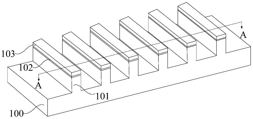
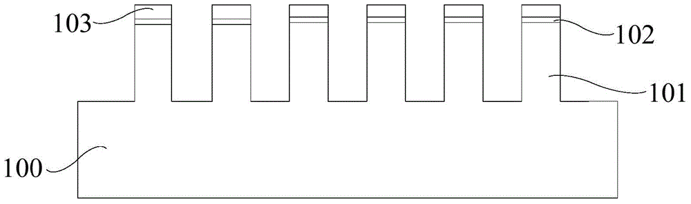
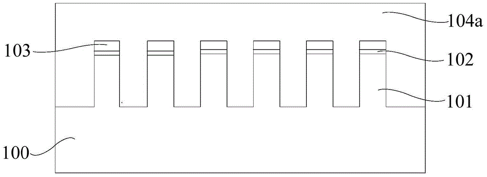
[0050] refer to Figure 5 , the material of the insulating material layer is silicon oxide. Wet etching is isotropic etching, and in the process of etching back the insulating material layer 104 a by wet etching, the pad oxide layer 102 made of the same material will also be corroded and broken. In this way, the mask layer 103 located on the pad oxide layer 102 will drop onto the insulating material layer 104a being wet-etched to form particles, which affect the formation quality of the insulating layer 104, for example, Holes appear in the insulating layer 104 , thereby affecting the isolation effect of the insulating layer 104 , and further affecting the performance of the subsequently formed FinFET.

[0051] Also, refer to Figure 6 to Figure 8 , because the mask layer 103 on the top of the fin 105 falls off, the channel stop ion implantation will be perfor...


PUM


Abstract

A fin field effect transistor and its forming method, wherein, the forming method of the fin field effect transistor includes: providing a semiconductor substrate, the semiconductor substrate has at least two discrete raised structures, on the raised structures having a pad oxide layer and a mask layer on the pad oxide layer; forming a barrier layer on sidewalls of the raised structure, sidewalls of the pad oxide layer, sidewalls and top of the mask layer; forming an insulating layer on the barrier layer between adjacent raised structures, the insulating layer being lower than the raised structures; trenching the mask layer, the pad oxide layer and the raised structures channel stop ion implantation to form a channel stop ion implantation layer. The performance of the fin field effect transistor can be improved by adopting the method of the invention.

Description

technical field [0001] The invention relates to the field of semiconductors, in particular to a fin field effect transistor and a forming method thereof. Background technique [0002] With the development of the semiconductor industry to lower technology nodes, the transition from planar CMOS transistors to three-dimensional Fin Field Effect Transistors (FinFETs) has gradually begun. In FinFET, the gate structure can control the channel from at least two sides, which has a much stronger gate-to-channel control ability than planar MOSFET devices, and can well suppress the short-channel effect. And compared with other devices, it has better compatibility with the existing integrated circuit production technology. [0003] refer to Figure 1 to Figure 7 , the forming method of the fin field effect NMOS transistor in the prior art is as follows: [0004] refer to figure 1 and figure 2 , providing a silicon substrate 100 with at least two discrete raised structures 101 on t...

Claims


Application Information

Patent Timeline
Patent Type & Authority Applications(China)
IPC IPC(8): H01L21/336H01L21/318H01L29/78H01L29/06
CPCH01L29/66795
Inventor 李勇赵海居建华
Owner SEMICON MFG INT (SHANGHAI) CORP
Why Eureka
Try Eureka