Electronic encapsulation structure

一种电子封装、电子元件的技术,应用在电路、印刷电路、电气元件等方向,能够解决整合难度高、导电硅穿孔100成本昂贵、技术难度高等问题

Active Publication Date: 2016-08-10
PHOENIX PIONEER TECH
View PDF5 Cites 24 Cited by
  • Summary
  • Abstract
  • Description
  • Claims
  • Application Information

AI Technical Summary

Problems solved by technology

[0018] However, in the existing photosensitive packaging structure 1", due to the high cost of making the conductive TSV 100, the difficulty of integration, and the high technical difficulty, especially the electronic components used in sensor components or camera lenses are all expensive.

Method used


Image

  • Electronic encapsulation structure
  • Electronic encapsulation structure
  • Electronic encapsulation structure

Examples


Embodiment Construction

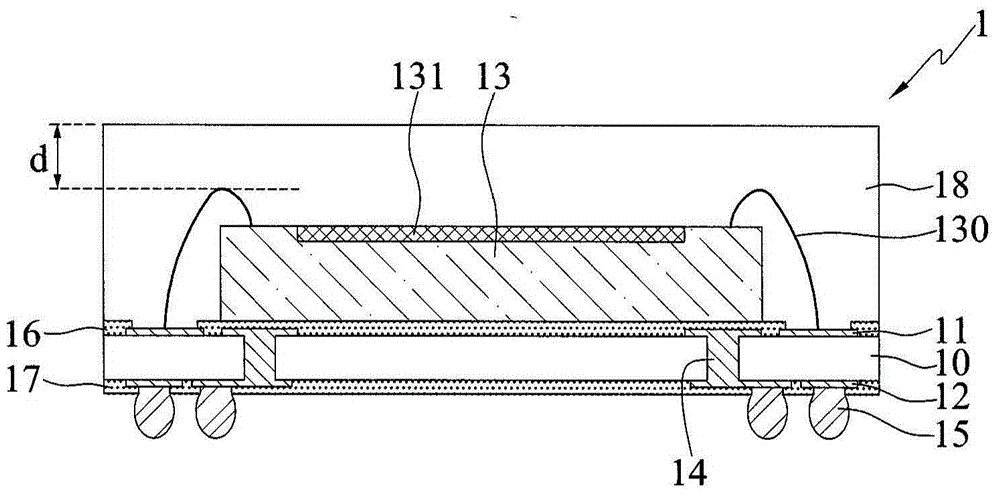
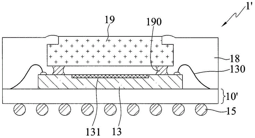
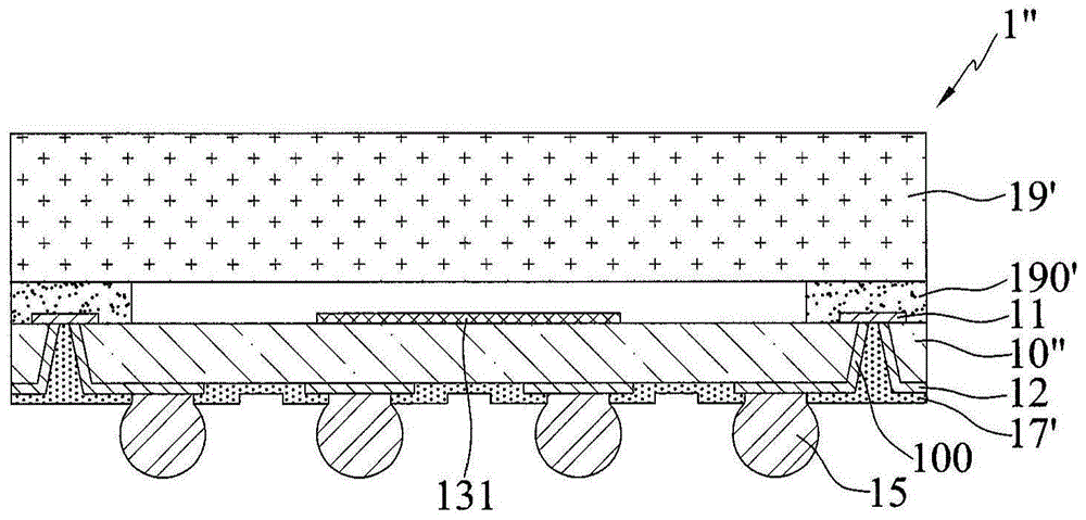
[0074] Embodiments of the present invention are described below through specific examples, and those skilled in the art can easily understand other advantages and effects of the present invention from the content disclosed in this specification.

[0075] It should be noted that the structures, proportions, sizes, etc. shown in the drawings attached to this specification are only used to match the content disclosed in the specification, for the understanding and reading of those skilled in the art, and are not used to limit the implementation of the present invention. Limiting conditions, so there is no technical substantive meaning, any modification of structure, change of proportional relationship or adjustment of size, without affecting the effect and purpose of the present invention, should still fall within the scope of the present invention. The disclosed technical content must be within the scope covered. At the same time, terms such as "above", "first", "second", and "o...


PUM


Abstract

An electronic encapsulation structure comprises an insulating layer, an electronic component which is embedded in the insulating layer and has an induction area exposed to the insulator, and a first circuit layer which is arranged on the insulating layer and electrically connected with the electronic component. Thus, the thickness of the whole encapsulation structure is reduced.

Description

technical field [0001] The invention relates to an electronic packaging structure, in particular to an electronic packaging structure that can be thinned. Background technique [0002] With the development of the electronic industry, today's electronic products have tended to be designed in the direction of thinner, smaller and more functional, and semiconductor packaging technology has also developed different packaging types. [0003] At present, most electronic components used in sensor components or camera lenses are still packaged by wire bonding or Chip On Board (COB for short). [0004] Such as Figure 1A As shown, the existing wire bonding package structure 1 includes: a substrate 10 , an electronic component 13 and a packaging compound 18 . [0005] The substrate 10 is provided with a first circuit layer 11 and a second circuit layer 12 on the upper and lower sides, and the first and second circuit layers are electrically connected through through holes or blind ho...

Claims


Application Information

Patent Timeline
Patent Type & Authority Applications(China)
IPC IPC(8): H01L23/12
CPCH01L2924/181H01L23/5389H05K1/185H05K2201/10121H05K2201/10151H01L27/14618H01L2224/48091H01L2224/48227H01L2924/15311H01L2924/16235H01L2224/45144H01L2224/48465H01L24/24H01L24/82H01L2924/16251H01L2924/16195H01L23/10H01L2224/24225H01L2924/16315G06V40/1318H01L2924/00012H01L2924/00014H01L2924/00015H01L2924/00H01L2224/18H05K2201/10H05K3/284
Inventor 胡竹青许诗滨
Owner PHOENIX PIONEER TECH
Why Eureka
Try Eureka