A high-speed intelligent cutting machine for chip electronic components

A technology of electronic components and cutting machines, applied in the direction of work accessories, manufacturing tools, stone processing equipment, etc., can solve the problem that there is no function of auto focus, automatic search for block marking points, and the camera does not have automatic adjustment and auto focus functions. High cutting accuracy and other issues, to achieve the effect of high consistency, high positioning accuracy, and small cutting resistance

Active Publication Date: 2018-05-04
肇庆市宏华电子科技有限公司
View PDF13 Cites 4 Cited by
  • Summary
  • Abstract
  • Description
  • Claims
  • Application Information

AI Technical Summary

Problems solved by technology

[0011] In the prior art ceramic diaphragm cutting machine, its feeding and receiving are manually operated, and it is difficult to align the blocks neatly, the cutting accuracy is reduced, and the efficiency is low
[0012] In the prior art ceramic diaphragm cutting machine, the camera in its detection and positioning mechanism has no automatic adjustment and auto-focus functions, which also reduces the cutting accuracy and is prone to the problem of cutting the wrong cutting line. The wrong cutting is: when aligning , the left side of the cutting knife is aligned with the first cutting line on the left side of the block, and the right side of the cutting knife is aligned with the second cutting line on the right side of the block. After cutting in this way, none of the thousands of products in the entire block is qualified, and all of them are invalid.
[0013] The patent inquired from the national patent network: chip multilayer ceramic capacitor inductance cutting machine, patent number 2003101077178, announcement number CN 1260049 C, introduces a machine frame, bearing plate, cutter mechanism, camera device and control system. The advanced cutting machine is manual feeding, the camera device does not have the function of auto-focusing and automatically finding the marking points of the block, and the forward and backward of the carrier plate uses an ordinary servo motor, which cannot achieve high cutting accuracy and the ability to cut small-sized products

Method used


Image

  • A high-speed intelligent cutting machine for chip electronic components
  • A high-speed intelligent cutting machine for chip electronic components
  • A high-speed intelligent cutting machine for chip electronic components

Examples


Embodiment Construction

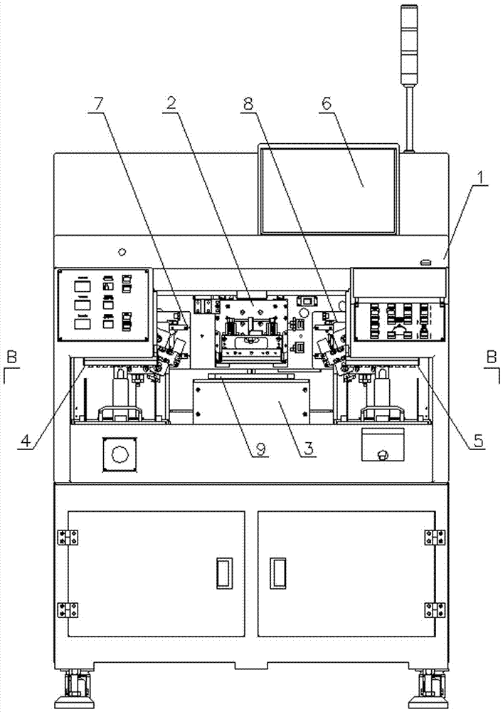
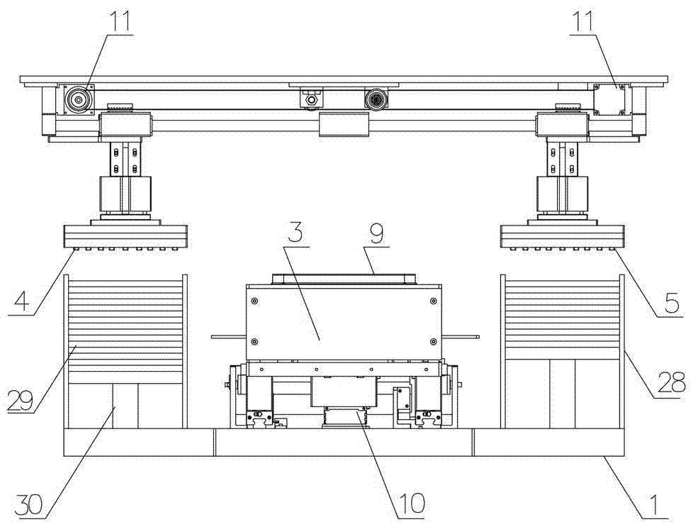
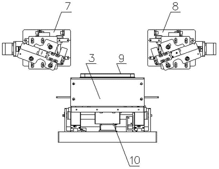
[0054] figure 1 It is a schematic diagram of a high-speed intelligent cutting machine for chip electronic components. Including the body structure 1, carrier 9, detection and positioning mechanism, cutting mechanism 2, control system, and operation panel 6, a vacuum channel is provided inside the carrier 9, and a feeding and receiving mechanism 5 is set above the left and right sides of the carrier 9 ,See figure 2 , the feeding and receiving mechanism 5 is provided with a vacuum suction cup and a feeding and receiving transmission motor, below the vacuum suction cup, a bar block warehouse for accessing the bar block 29 is set, and in the body structure 1 at the bottom of the bar block storehouse, there is a The electric ejector rod 30 of bar block 29 displacements up and down, see Figure 4 , 5 , the lower part of the carrier 9 is connected to the carrier plate 3, and at the junction of the carrier 9 and the carrier 3, there is a DD direct drive servo rotation mechanism 33...


PUM

PropertyMeasurementUnit
thicknessaaaaaaaaaa

Abstract

The invention relates to a high-speed intelligent cutting machine for chip-type electronic components in the field of manufacturing devices for electronic components. The high-speed intelligent cutting machine comprises a machine body structure, a bearing table, a detection locating mechanism, a cutting mechanism and a control system, wherein a feeding mechanism and a collecting mechanism comprising vacuum sucking discs, conveying motors and block bins are arranged on the left and right sides of the bearing table; electric ejector rods are arranged at the bottoms of the block bins; a bearing plate is connected at the lower part of the bearing table; a DD direct drive servo rotating mechanism capable of enabling the bearing table to rotate relative to the bearing plate is arranged at the middle connection part of the bearing table and the bearing plate; a linear drive servo motor capable of enabling the bearing plate to perform linear motion front and back is arranged below the bearing plate; and the detection locating mechanism is a CCD detector, and is provided with a motor which can drive the CCD detector to move, search block mark points and automatically focus. According to the high-speed intelligent cutting machine, the automatic feeding mechanism and the collecting mechanism are arranged, and manual operation is replaced, so that the product quality is improved; and the CCD detector, the DD direct drive servo rotating mechanism and the linear drive servo motor achieve automatic alignment detection, the detection is accurate, the recognition is intelligent, the cutting accuracy is high, and products with small sizes can be cut.

Description

technical field [0001] The invention relates to the field of electronic component manufacturing equipment, in particular to a high-speed intelligent cutting machine for chip electronic components. Background technique [0002] There are more and more varieties of electronic products, with increasingly powerful functions and smaller and smaller volumes. This requires that the main electronic components in the manufacture of electronic products, such as capacitors, resistors, inductors, sensors, etc., should be as small as possible and as reliable as possible. At present, only chip ceramic electronic components can meet the above requirements at the same time. Ceramic electronic components are calcined at a high temperature above 1000°C, and their insulation, heat resistance, durability and other aspects all show excellent performance. As a result, the manufacture, sale and use of chip ceramic electronic components have flourished. [0003] The process of producing chip cera...

Claims


Application Information

Patent Timeline
Patent Type & Authority Patents(China)
IPC IPC(8): B28D1/22B28D7/00B28D7/04
CPCB28D1/222B28D7/00B28D7/04
Inventor 梁耀国梁国衡唐忠辉江玉娟何海华李焕俊胡志安
Owner 肇庆市宏华电子科技有限公司
Why Eureka
Try Eureka