

Conducting cylinder, manufacturing method thereof, chip packaging method and flip chip product
A conductor post and chip technology, which is used in semiconductor/solid-state device manufacturing, semiconductor devices, and semiconductor/solid-state device components, etc. Failure and other problems, to achieve the effect of not easy to fail or circuit failure, excellent robustness, good uniformity and compactness
- Summary
- Abstract
- Description
- Claims
- Application Information
AI Technical Summary
Problems solved by technology
Method used
Image

Examples
no. 1 example
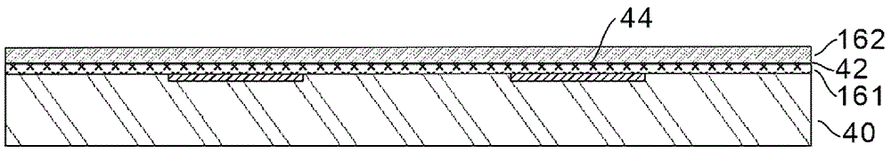
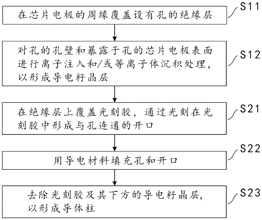
[0068] figure 2 It is a flowchart showing a method of manufacturing a conductor post according to the first embodiment of the present invention. The method involves forming a conductor post on the surface of the chip electrode, and includes the following steps: covering the periphery of the chip electrode with an insulating layer provided with a hole (step S11); performing the hole wall of the hole and the surface of the chip electrode exposed to the hole Ion implantation and / or plasma deposition treatment to form a conductive seed layer (step S12); cover the insulating layer with photoresist, and form openings in the photoresist that communicate with the holes by photolithography (step S21); The conductive material fills the holes and openings (step S22); and, the photoresist and the conductive seed layer underneath are removed to form a conductive pillar (step S23). Among them, steps S11 and S12 correspond to figure 1 Step S1 is shown, and steps S21, S22, and S23 correspond ...
no. 2 example
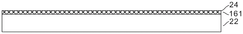
[0081] Image 6 It is a flowchart showing a method of manufacturing a conductor post according to the second embodiment of the present invention. The method involves forming a conductor post on the hole wall of a hole formed in a chip, and includes the following steps: drilling a through hole on a chip or two or more chips stacked together, and covering an insulating layer around the through hole ( Step S11); ion implantation and / or plasma deposition are performed on the wall of the through hole to form a conductive seed layer that penetrates a chip or two or more chips stacked together (step S12); conductive material is used Fill the via hole (step S21); and remove the insulating layer to form a conductor post (step S22). Among them, steps S11 and S12 correspond to figure 1 Step S1 is shown, while steps S21 and S22 correspond to figure 1 Shown in step S2. In addition, Figure 7(a)-(d) is a diagram showing the difference between Image 6 The corresponding structural cross-secti...
no. 3 example
[0087] Figure 8 It is a flowchart showing a method of manufacturing a conductor post according to the third embodiment of the present invention. The method involves forming conductor posts on the circuit surface of the packaging substrate, and includes the following steps: ion implantation and / or plasma deposition treatment is performed on the surface of the packaging substrate to form a conductive seed layer (step S1); on the packaging substrate Cover the photoresist, and form an opening in the photoresist by photolithography to expose the circuit surface of the package substrate (step S21); fill the opening with a conductive material (step S22); remove the photoresist and the conductive seed layer underneath, To form a conductor post (step S23). Among them, steps S21, S22 and S23 correspond to figure 1 Shown in step S2. In addition, Fig. 9(a)-(d) shows the difference between Figure 8 The corresponding structural cross-sectional schematic diagrams of each step of the method...
PUM
| Property | Measurement | Unit |
|---|---|---|
| Thickness | aaaaa | aaaaa |
Abstract
Description
Claims
Application Information