ZnS nanobelt/CdS nanorod heterojunction synthetic method

A synthesis method and nano-column technology, applied in sustainable manufacturing/processing, electrical components, climate sustainability, etc., to achieve the effect of simple experimental scheme, low cost, and strong experimental repeatability

Inactive Publication Date: 2016-09-07
GUIZHOU UNIV
View PDF1 Cites 1 Cited by
  • Summary
  • Abstract
  • Description
  • Claims
  • Application Information

AI Technical Summary

Problems solved by technology

However, there are few reports on the synthesis of ZnS / CdS nanomaterial heterojunctions

Method used


Image

  • ZnS nanobelt/CdS nanorod heterojunction synthetic method
  • ZnS nanobelt/CdS nanorod heterojunction synthetic method

Examples


Embodiment 1

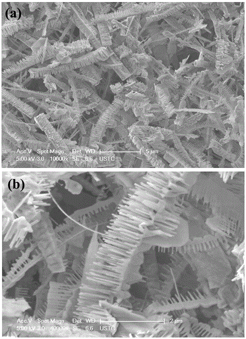
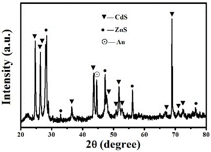
[0015] The first step: use an ion sputtering device to plate an Au film with a thickness of about 100nm on a silicon wafer (100 crystal orientation, 0.9cm*0.9cm), and use this coated silicon wafer as a catalyst. Step 2: Push the ceramic boat containing 0.7g ZnS powder into the quartz tube to the position of the thermocouple of the tube furnace, and then push the above-mentioned substrate into the quartz tube to a place 15cm away from the lower tuyere of the ceramic boat. Afterwards, argon gas was introduced for 30 minutes to discharge the oxygen present in the quartz tube. Under the protection of argon, the reaction temperature was raised from room temperature to 900°C and reacted at this temperature for 2 hours. After the whole device was cooled to room temperature, it could be observed that A certain amount of white sample was deposited on the substrate. Step 3: Place the ceramic boat containing 0.1g of CdS powder at the position of the thermocouple, and place the white samp...

Embodiment 2

[0019] The first step: use an ion sputtering device to plate an Au film with a thickness of about 120 nm on a silicon wafer (100 crystal orientation, 0.9 cm*0.9 cm), and use this coated silicon wafer as a catalyst. Step 2: Push the ceramic boat containing 0.75g of ZnS powder into the quartz tube to the position of the tube furnace thermocouple, and then push the above-mentioned substrate into the quartz tube to a distance of 16 cm from the lower tuyere of the ceramic boat. Afterwards, argon was introduced for 30 minutes to discharge the oxygen present in the quartz tube. Under the protection of argon, the reaction temperature was raised from room temperature to 920°C and reacted at this temperature for 2.5 hours. After the whole device was cooled to room temperature, it could be observed A certain amount of white sample was deposited on the substrate. Step 3: Place the ceramic boat containing 0.1g of CdS powder at the position of the thermocouple, and place the white sample pr...

Embodiment 3

[0021] The first step: use an ion sputtering device to plate an Au film with a thickness of about 80nm on a silicon wafer (100 crystal orientation, 0.9 cm*0.9 cm), and use this coated silicon wafer as a catalyst. The second step: push the ceramic boat containing 0.65g ZnS powder into the quartz tube to the position of the thermocouple of the tube furnace, and then push the above-mentioned substrate into the quartz tube to a distance of 17cm from the lower tuyere of the ceramic boat. Afterwards, argon gas was introduced for 30 minutes to discharge the oxygen present in the quartz tube. Under the protection of argon, the reaction temperature was raised from room temperature to 880 ° C and reacted at this temperature for 1.5 hours. After the whole device was cooled to room temperature, it could be observed that A certain amount of white sample was deposited on the substrate. Step 3: Place the ceramic boat containing 0.1g of CdS powder at the position of the thermocouple, and plac...


PUM

PropertyMeasurementUnit
thicknessaaaaaaaaaa

Abstract

The invention discloses a ZnS nanobelt / CdS nanorod heterojunction synthetic method, and the method is characterized in that the method comprises the following steps: firstly depositing a gold film on a silicon substrate through employing an ion sputtering instrument, putting ZnS powder into a ceramic boat, and placing the ceramic boat at the position of a pipe-type thermocouple; secondly placing the silicon substrate in a downwind direction of the ZnS powder, letting in argon gas, increasing the reaction temperature to 900+ / -20 DEG C under the protection of the argon gas, and carrying out reaction for 2+ / -0.5h under the temperature, wherein a white sample can be seen on the silicon substrate after the reaction; finally opening a device, placing the CdS powder at the position of the thermocouple, placing the white sample at a downwind port of the ZnS powder, increasing the reaction temperature to 800+ / -20 DEG C under the protection of the argon gas, carrying out reaction for 1+ / -0.3h at the temperature under the protection of argon gas, decreasing the temperature to the indoor temperature after the reaction is completed, and obtaining a flaxen sample on the silicon substrate.

Description

technical field [0001] The invention is a method for synthesizing II-VI semiconductor heterojunction materials (ZnS nanobelt / CdS nanocolumn heterojunction). Background technique [0002] II-VI compound semiconductors have been playing an important role in lasers, light-emitting diodes, solar cells and other applications due to their remarkable characteristics such as wide bandgap range, direct transition type energy band structure and rich luminescent colors. Nano-scale II-VI semiconductor materials show great application potential in the field of nano-optoelectronic devices because of their unique luminescent properties, semiconductor quantization performance and better meeting the needs of device miniaturization. Therefore, research on the synthesis, optoelectronic properties and applications of II-VI semiconductor nanomaterials has attracted people's attention in recent years. ZnS and CdS are representative II-VI semiconductor materials, and the research on these two nan...

Claims


Application Information

Patent Timeline
Patent Type & Authority Applications(China)
IPC IPC(8): H01L31/18
CPCH01L31/0296Y02P70/50
Inventor 祁小四谢忍白忠臣钟伟都有为
Owner GUIZHOU UNIV
Why Eureka
Try Eureka