Fuse Structure

A technology of fuse structure and fuse link, which is applied in the direction of electrical components, electric solid devices, circuits, etc., can solve the problems of circuit short circuit, small contact area, etc., and achieve the effect of reducing current density and strengthening electron migration ability

Inactive Publication Date: 2016-09-21
TAIWAN SEMICON MFG CO LTD
View PDF4 Cites 0 Cited by
  • Summary
  • Abstract
  • Description
  • Claims
  • Application Information

AI Technical Summary

Problems solved by technology

However, when large currents pass through the fuse, problems arise in the cathode contact window of conventional fuses, which are usually aligned with the axis of the fuse link and close to the fuse link, and have a very small contact area, Because the traditional cathode contact is close to and aligned with the fuse, the resistance between the fuse and the cathode contact is much lower than any resistance between the fuse and any other contact in the cathode, so this low resistance makes most The current flows through the cathode contact window
[0005] Large currents flowing through the cathode contact cause electrons from the metal in the contact to migrate to the fuse, and then when the high current attempts to create a more resistive path or open a circuit, the electron migration of the metal causes the fuse to short the circuit again
This problem will increase after the high temperature storage (high temperature storage; HTS) or baking process of the chip. Therefore, the industry urgently needs a more robust and durable fuse structure to overcome the defects of the known technology

Method used


Image

  • Fuse Structure
  • Fuse Structure
  • Fuse Structure

Examples


Embodiment Construction

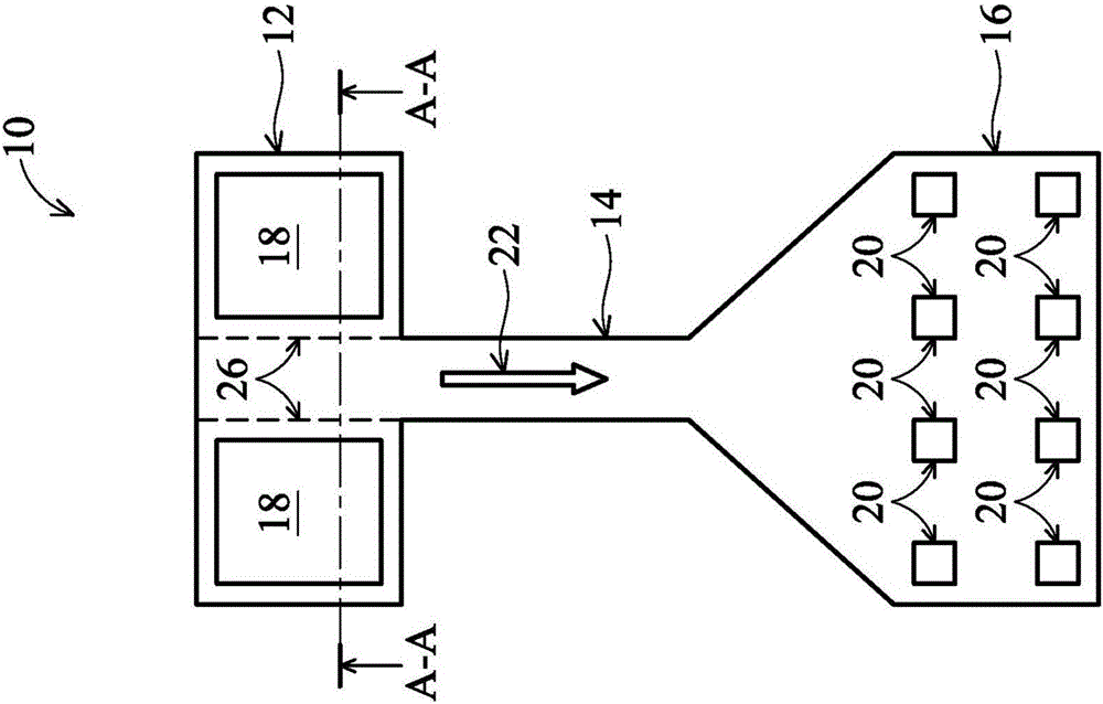
[0025] Embodiments described herein relate to e-fuse structures in semiconductor chips, but e-fuse structures may also be used in other embodiments.

[0026] figure 1 A fuse structure 10 is shown including a cathode 12 , a fuse link 14 and an anode 16 . The fuse structure 10 can be made of metal, such as copper or similar metal materials, or made of polysilicon silicide (silicided polysilicon), such as nickel silicon (NiSi), titanium silicon (TiSi 2 ), cobalt silicon (CoSi x ), platinum silicon (PtSi 2 ) or similar material. The cathode 12 has a rectangular upper surface, and two contacts 18 are coupled to the upper surface. Anode 16 has a funnel-shaped upper surface, and contact window 20 is coupled to the upper surface. Contacts 18 and 20 may include copper, tungsten, or similar metals, and may also include a diffusion barrier layer including, for example, TiN, TaN, or similar material lined within contacts 18 and 20 . The width of fuse 14 (perpendicular to arrow 22 ) ...


PUM


Abstract

An embodiment is a fuse structure. In accordance with an embodiment, the fuse structure comprises an anode, a cathode, a fuse link interposed between the anode and the cathode, and cathode connectors coupled to the cathode. The cathode connectors are each equivalent to or larger than about two times a minimum feature size of a contact that couples to an active device. The fuse structure is firmer and more durable, can reduce large currents isolated in well-known single contacts, and has greater electron transfer capability, so that metal in or above contacts cannot be transferred to a fuse link and cause short circuit of the fuse structure.

Description

[0001] The application date is October 18, 2010, the application number is 201010514753.6, the priority date is October 30, 2009, April 30, 2010 and February 26, 2010, and the invention name is "fuse structure "A divisional application of the invention patent application. technical field [0002] The present invention relates to a fuse structure and its forming method, in particular to an electric fuse in a semiconductor element and its forming method. Background technique [0003] In the semiconductor industry, fuse elements are widely used in integrated circuits for various purposes, such as memory repair, analog resistor adjustment, and chip identification. For example, replacing defective memory cells with redundant memory cells on the same chip can significantly increase memory manufacturing yields. A fuse that is cut by a laser beam is called a laser fuse, and a fuse that is cut or blown by passing an electric current is called an electrical fuse or an e-fuse. By sel...

Claims


Application Information

Patent Timeline
Patent Type & Authority Applications(China)
IPC IPC(8): H01L23/525
CPCH01L23/5256H01L23/5226H01L2924/0002H01L2924/00
Inventor 吴显扬龚威菖
Owner TAIWAN SEMICON MFG CO LTD
Why Eureka
Try Eureka