Eureka AIR delivers breakthrough ideas for toughest innovation challenges, trusted by R&D personnel around the world.

Super-junction power device and manufacturing method thereof

A technology for power devices and manufacturing methods, applied in the fields of semiconductor/solid-state device manufacturing, semiconductor devices, electrical components, etc., can solve problems such as reducing the breakdown voltage of devices, and achieve the effects of reducing leakage, convenient setting, and good impact resistance.

Active Publication Date: 2016-09-21
SHANGHAI HUAHONG GRACE SEMICON MFG CORP
View PDF5 Cites 16 Cited by
  • Summary
  • Abstract
  • Description
  • Claims
  • Application Information

AI Technical Summary

Problems solved by technology

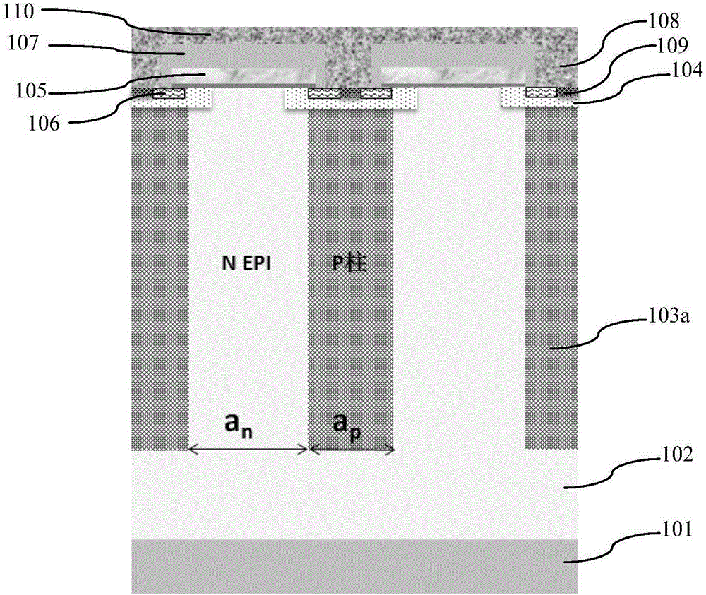
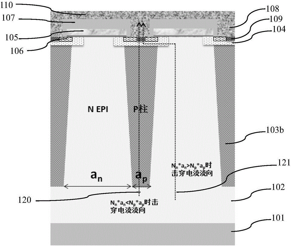
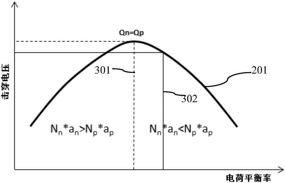
figure 2 In the structure shown in the actual situation, the reason why the charge balance rate is set in the coordinate area where the abscissa is greater than the dotted line 301 is to ensure that the device has the final impact resistance. figure 2 The arrow in dashed line 120 corresponds to the charge balance rate N n ×a n p ×a p When the breakdown current flows, it is obvious that the breakdown current passes through the P-type column 103b; the arrow dotted line 121 corresponds to the charge balance rate of N n ×a n >N p ×a p When the breakdown current flows, it is obvious that the breakdown current passes through the N-type pillar; when the breakdown current passes through the P-type pillar 103b, it has greater impact resistance. The charge balance rate is set at N n ×a n p ×a p region, but this reduces the breakdown voltage of the device

Method used


Image

  • Super-junction power device and manufacturing method thereof
  • Super-junction power device and manufacturing method thereof
  • Super-junction power device and manufacturing method thereof

Examples


Embodiment Construction

[0053] Such as Figure 4 What is shown is a schematic structural diagram of a super junction power device in an embodiment of the present invention; the super junction power device in an embodiment of the present invention includes:

[0054] A semiconductor substrate such as a silicon substrate 1, an N-type epitaxial layer 2 such as an N-type silicon epitaxial layer 2 is formed on the surface of the semiconductor substrate 1; a plurality of trenches are formed on the N-type epitaxial layer 2, and the trenches are filled There are P-type pillars 4, and the P-type pillars 4 filled in the trenches and the N-type pillars composed of the N-type epitaxial layer 2 between the trenches are alternately arranged to form a super junction structure.

[0055] The side surface of the trench has an inclined structure and the bottom width of the trench is smaller than the top width, so as to facilitate the etching and filling of the trench.

[0056] A doping compensation layer 3 formed by ion implan...


PUM


Abstract

The invention discloses a super-junction power device. A super-junction structure is formed on an N-type epitaxial layer; each groove is filled with a P-type post in the super-junction structure; the side surface of each groove is of an inclined structure to facilitate etching and filling of the groove; a doping compensation layer formed through ion implantation is formed on the side surface of each groove; and the doping concentration of each doping compensation layer in the direction from the top part of the corresponding groove to the bottom part is gradually changed for compensating the influence of the widths of the grooves at different depths on the charge balance of the P-type posts and N-type posts, so that the charge balance of the P-type posts at different depths of the grooves and the adjacent N-type posts is improved to improve the puncture voltage of the super-junction power device. The invention further discloses a manufacturing method of the super-junction power device. The puncture voltage of the super-junction structure with the inclined structures on the side surfaces of the grooves can be improved; and meanwhile, the device can also has good anti-impact ability.

Description

Technical field [0001] The invention relates to the field of semiconductor integrated circuit manufacturing, in particular to a super junction power device; the invention also relates to a method for manufacturing a super junction power device. Background technique [0002] The super junction structure is a structure composed of alternately arranged N-type pillars and P-type pillars. If a super junction structure is used to replace the N-type drift region in a vertical double-diffused metal-oxide-semiconductor (VDMOS) device, the conduction path is provided through the N-type pillar in the conduction state. The P-type pillar does not provide a conduction path; in the off state, the PN pillar jointly bears the reverse bias voltage to form a superjunction metal-oxide-semiconductor field-effect transistor (Metal-Oxide-Semiconductor Field-Effect Transistor, MOSFET). Super-junction MOSFET can greatly reduce the on-resistance of the device by using a low-resistivity epitaxial layer un...

Claims


Application Information

Patent Timeline
Patent Type & Authority Applications(China)
IPC IPC(8): H01L29/78H01L29/739H01L29/06H01L29/36H01L21/336H01L21/331
CPCH01L29/0634H01L29/0684H01L29/36H01L29/66333H01L29/66666H01L29/7395H01L29/7827H01L29/7802
Inventor 柯行飞
Owner SHANGHAI HUAHONG GRACE SEMICON MFG CORP
Why Eureka
Eureka Blog
Learn More