A kind of conductive thin film manufacturing method and conductive thin film
A manufacturing method and technology of conductive film, which are applied in the direction of cable/conductor manufacturing, conductive layer on insulating carrier, circuit, etc., can solve the problems affecting the performance of MEMS microphone, thickness and stress that do not meet requirements, etc.
- Summary
- Abstract
- Description
- Claims
- Application Information
AI Technical Summary
Problems solved by technology
Method used
Image

Examples
Embodiment 1
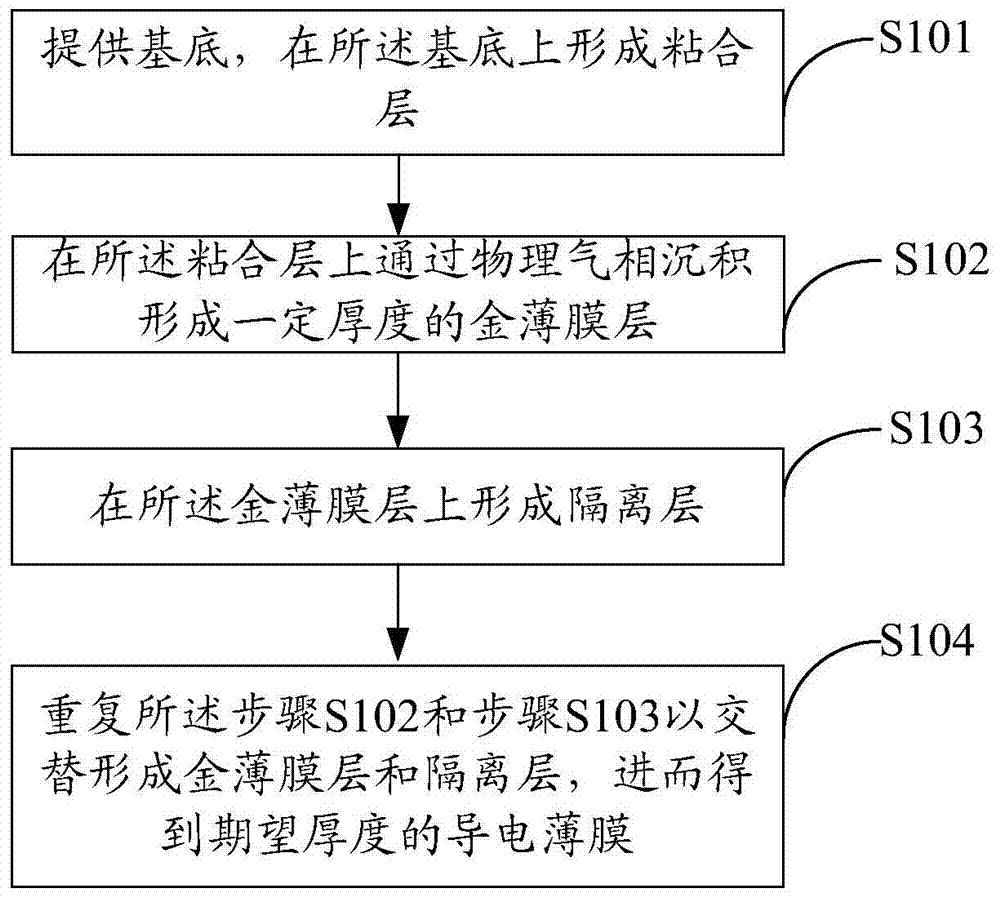
[0039] Combine below Figure 2A ~ Figure 2C A method for fabricating a metal thin film according to an embodiment of the present invention is described in detail.
[0040] In this embodiment, a PVD machine that can install targets of up to 4 materials in one process chamber and process 6 wafers at the same time is used, so both Cr and Au targets are installed in this machine , the deposition of the entire sandwich structure can be completed in the same chamber, the specific process is:
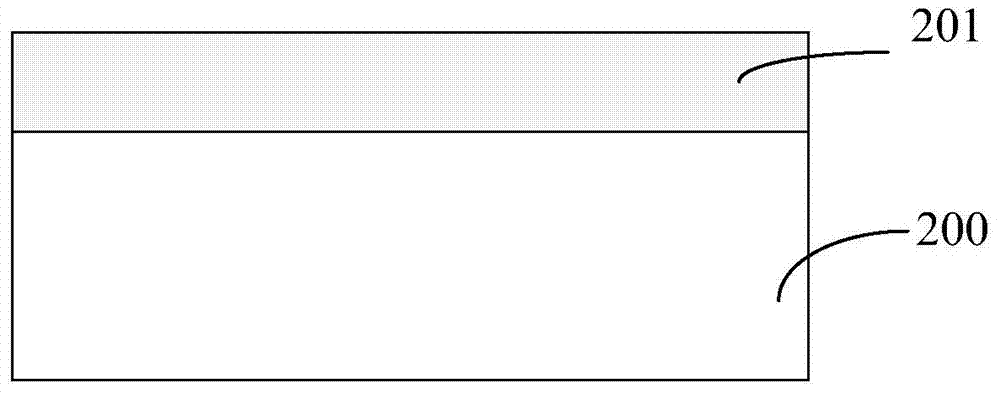
[0041] First, if Figure 2A As shown, a substrate 200 is provided, and an adhesive layer 201 is formed on the substrate 200 .
[0042] The substrate 200 plays a supporting role, and a silicon nitride film or a silicon dioxide film with a suitable thickness can be used, and the substrate 200 can be formed on a suitable wafer. Adhesive layer 201 plays a role in improving the deposition performance and facilitates the deposition of the subsequent conductive film. It can be selected from materi...
Embodiment 2
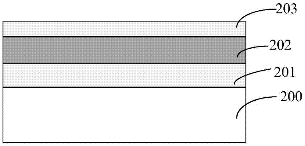
[0051] The present invention also provides a conductive thin film 100 made by the method described in Embodiment 1, which includes a substrate 300, an adhesive layer 301 on the substrate 300, and alternately formed gold thin film layers on the adhesive layer 301 ( 302, 304, 306) and isolation layers (303, 305), wherein the gold thin film layer (302, 304, 306) is formed by physical vapor deposition, and the gold thin film layer is obtained by controlling the process parameters of physical vapor deposition The required stress, the process parameters include one or more of radio frequency power, air flow rate and tray rotation speed.
[0052] In this implementation, the substrate 300 is made of silicon nitride or silicon oxide, which plays the role of supporting the conductive film, and the adhesive layer 301 plays the role of facilitating the deposition of the metal film layer. The cr layer is used as the adhesive layer, and of course other material layers with appropriate thic...
PUM
 Abstract
Description
Claims
Application Information
 - R&D
- Intellectual Property
- Life Sciences
- Materials
- Tech Scout
- Unparalleled Data Quality
- Higher Quality Content
- 60% Fewer Hallucinations
Browse by: Latest US Patents, China's latest patents, Technical Efficacy Thesaurus, Application Domain, Technology Topic, Popular Technical Reports.
© 2025 PatSnap. All rights reserved.Legal|Privacy policy|Modern Slavery Act Transparency Statement|Sitemap|About US| Contact US: help@patsnap.com