Electromagnetic shielding film
A technology of electromagnetic shielding film and conductive adhesive layer, which is applied in the fields of magnetic field/electric field shielding, electrical components, layered products, etc., and can solve the problem of electromagnetic shielding film taking into account solder resistance, adhesive strength, and metal layer fracture of electromagnetic shielding film at the same time , Electromagnetic shielding film is easy to delaminate and other problems, to achieve the effect of high adhesion, excellent solder resistance, excellent corrosion resistance
- Summary
- Abstract
- Description
- Claims
- Application Information
AI Technical Summary
Problems solved by technology
Method used
Image


Examples
preparation example Construction
[0028] The preparation process of the electromagnetic shielding film is not particularly limited in the present invention, it can be prepared according to the preparation process of the electromagnetic shielding film well known to those skilled in the art, and can be prepared according to the following process:
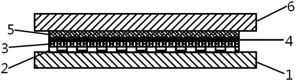
[0029] a), coating the first insulating layer material on one side of the carrier layer material, and curing to obtain the first insulating layer arranged on one side of the carrier layer; the carrier layer material is preferably a PET film; the first insulating layer The material includes polyimide resin, and preferably also includes heat-conducting material and / or light-absorbing material; the curing temperature is preferably 120-200°C; the curing time is preferably 30-120s.
[0030] b) coating a second insulating layer material on the surface of the first insulating layer and curing it to obtain a second insulating layer disposed on the surface of the first insulati...
Embodiment 1
[0038] 1) Raw materials:
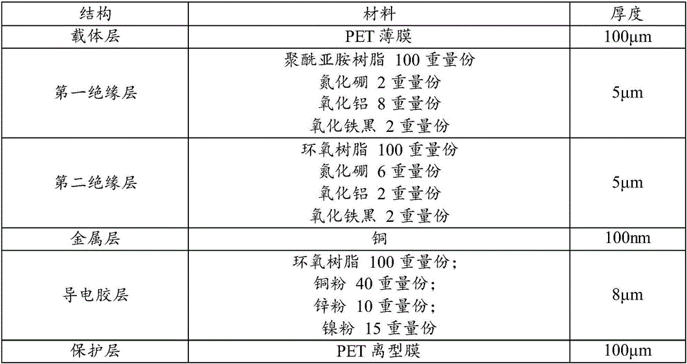
[0039] PET film (number-average molecular weight 50,000-120,000, thickness 20 μm); polyimide resin (sp-f1 polyimide resin from DuPont, USA); boron nitride (particle size ≤ 3 μm); alumina (particle size diameter≤3μm); iron oxide black (particle size≤3μm); epoxy resin (number average molecular weight 10000-30000, viscosity at 21°C 3000-7000cps); copper powder (particle diameter 1-5μm); nickel powder (particle size 1-5μm); PET release film (single-sided silicone oil release film, number average molecular weight 50,000-120,000, thickness 20μm, release force 5-10gf).
[0040] 2) Electromagnetic shielding film specifications, as shown in Table 1:
[0041] The electromagnetic shielding film specification that table 1 embodiment 1 provides
[0042]
[0043] 3) Preparation of electromagnetic shielding film:
[0044] According to the design specifications of the above electromagnetic shielding film, the electromagnetic shielding film is prepared; first, ...
Embodiment 2
[0046] 1) Raw materials:
[0047] PET film (number-average molecular weight 50,000-120,000, thickness 100 μm); polyimide resin (sp-f1 polyimide resin from DuPont, USA); boron nitride (particle size ≤ 3 μm); alumina (particle size diameter≤3μm); iron oxide black (particle size≤3μm); epoxy resin (number average molecular weight 10000-30000, viscosity at 21°C 3000-7000cps); copper powder (particle diameter 1-5μm); nickel powder (particle size 1-5μm); PET release film (single-sided silicone oil release film, number average molecular weight 50,000-120,000, thickness 100μm, release force 5-10gf).
[0048] 2) Electromagnetic shielding film specifications, as shown in Table 2:
[0049] The electromagnetic shielding film specification that table 2 embodiment 2 provides
[0050]
[0051] 3) Preparation of electromagnetic shielding film:
[0052] According to the design specifications of the above electromagnetic shielding film, the electromagnetic shielding film is prepared; first...
PUM
| Property | Measurement | Unit |
|---|---|---|
| thickness | aaaaa | aaaaa |
| peel strength | aaaaa | aaaaa |
| electrical resistance | aaaaa | aaaaa |
Abstract
Description
Claims
Application Information
 - R&D
- Intellectual Property
- Life Sciences
- Materials
- Tech Scout
- Unparalleled Data Quality
- Higher Quality Content
- 60% Fewer Hallucinations
Browse by: Latest US Patents, China's latest patents, Technical Efficacy Thesaurus, Application Domain, Technology Topic, Popular Technical Reports.
© 2025 PatSnap. All rights reserved.Legal|Privacy policy|Modern Slavery Act Transparency Statement|Sitemap|About US| Contact US: help@patsnap.com