Epoxy resin composition and semiconductor device

a technology of epoxy resin and semiconductor devices, applied in semiconductor devices, solid-state devices, basic electric elements, etc., can solve the problems of reducing reliability, affecting the performance of semiconductor devices, and affecting the reliability of semiconductor devices, and achieve good soldering resistan

Inactive Publication Date: 2005-04-21
SUMITOMO BAKELITE CO LTD
View PDF1 Cites 9 Cited by
  • Summary
  • Abstract
  • Description
  • Claims
  • Application Information

AI Technical Summary

Benefits of technology

[0010] From one of the viewpoints, a object of the invention is to provide an epoxy resin composition and a semiconductor device exhibiting good soldering resistance in which peeling from a lead frame does not occur during soldering after moisture absorption.
[0018] A semiconductor device prepared using an epoxy resin composition of the present invention has a characteristic that peeling from a lead frame is prevented even during soldering after moisture absorption, resulting in reliable resistance to soldering. The epoxy resin composition of this invention can be, therefore, extensively used for a variety of resin encapsulating type semiconductor devices. In particular, significant improvement can be achieved in adhesiveness between a cured resin composition and a plated lead frame (e.g., a silver-plated lead frame, a nickel-plated lead frame, a pre-plating frame in which a nickel / palladium alloy is plated with gold). Thus, the composition can be suitably used in a semiconductor device using a plated lead frame.
[0019] Since the epoxy resin composition of the present invention has a characteristic that peeling from a lead frame is prevented even during soldering after moisture absorption, a semiconductor device prepared using the composition is reliably resistant to soldering.

Problems solved by technology

In surface mounting for such a semiconductor device, the semiconductor device is suddenly exposed to an elevated temperature of 200° C. or higher during a solder dipping or solder reflow process, leading to explosive vaporization of absorbed moisture.
Such vaporization may generate a sufficient stress to cause peeling in an interface between each plated junction on a semiconductor element, lead frame or inner lead and a cured epoxy resin composition, or cracks in a semiconductor device, leading to significantly lower reliability.
When adhesive strength in the interface is weak, peeling may occur in the interface between the cured epoxy resin composition and the base material after soldering, leading to cracks in the semiconductor device.
However, these silane coupling agents alone have become inadequate to meet more strict requirement in soldering resistance in association with a higher reflow temperature during mounting and the use of a pre-plating frame made of Ni, Ni—Pd or Ni—Pd—Au in response to a lead-free solder.
However, the silane coupling agent described in Japanese Laid-open Patent Application No. 1994-350000 has a drawback that it is unstable at an elevated temperature, leading to insufficiently improved adhesion after soldering resistance treatment.

Method used


Image

  • Epoxy resin composition and semiconductor device
  • Epoxy resin composition and semiconductor device
  • Epoxy resin composition and semiconductor device

Examples


experimental example 1

[0037] An epoxy resin represented by formula (2) (softening point: 58° C., epoxy equivalent: 272; hereinafter, referred to as “Epoxy resin 1”): 8.2 parts by weight

[0038] A phenolic resin represented by formula (3) (softening point: 107 degrees centigrade, hydroxy equivalent: 200; hereinafter, referred to as “Phenolic resin 1”): 6.0 parts by weight

[0039] An equivalent ratio of epoxy groups in the total epoxy resins to phenolic hydroxy groups in the total phenolic resins is calculated as 1.0.

[0040] 1,8-Diazabicyclo[5.4.0]undecene-7 (hereinafter, referred to as “DBU”): 0.2 parts by weight.

[0041] Spherical fused silica (Micron Co., Ltd., average particle size: 28 Mm): 85.0 parts by weight.

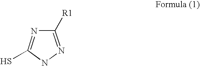
[0042] 1,2,4-Triazole-5-thiol represented by formula (4) (Reagent Grade): 0.1 parts by weight [0043] Carnauba wax: 0.2 parts by weight [0044] Carbon black: 0.3 parts by weight.

[0045] These components were mixed using a mixer, kneaded using two rolls with surface temperature of 90 degrees centi...

experimental examples 2 to 15

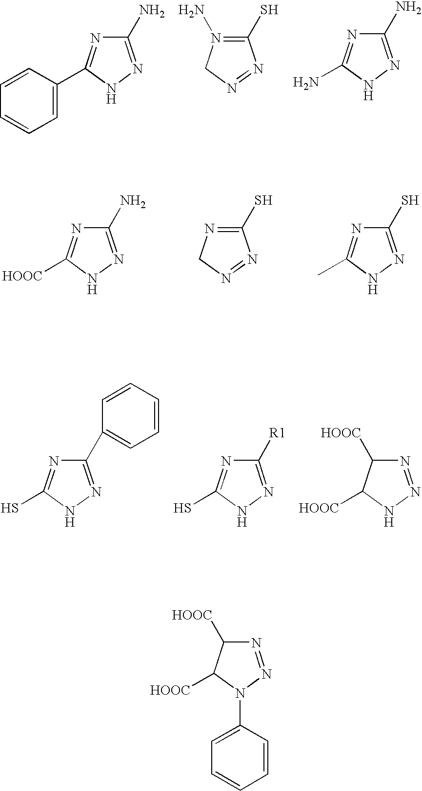
[0049] According to blending rates in Tables 1 and 2, epoxy resin compositions were prepared and evaluated as described in Experimental Example 1. The results are shown in Tables 1 and 2. Specific epoxy resins and phenolic resins used are shown in Table 3. Triazole compounds used in the experiments other than Experimental Example 1 are as follows.

[0050] 3-Amino-1,2,4-triazole-5-thiol represented by formula (5) (Reagent grade)

[0051] 3,5-Dimercapto-1,2,4-triazole represented by formula (6) (Reagent grade).

[0052] 3-Hydroxy-1,2,4-triazole-5-thiol represented by formula (7) (Reagent grade).

[0053] 5-Mercapto-1,2,4-triazole-3-methanol represented by formula (8) (Reagent grade).

[0054] 2-(4′-Morpholinodithio)benzothiazole represented by formula (9) (Kawaguchi Chemical Industry Co,. Ltd.).

TABLE 1Experimental Examples123456789101112Epoxy resin 18.28.28.28.28.27.16.5Epoxy resin 27.47.47.47.47.4Phenolic resin 16.06.06.06.06.05.24.8Phenolic resin 26.86.86.86.86.8(Equivalent ratio of ep...


PUM

PropertyMeasurementUnit
temperatureaaaaaaaaaa
surface temperatureaaaaaaaaaa

Abstract

One of major objects of the invention is to provide an epoxy resin composition and a semiconductor device exhibiting good soldering resistance when being formed on a non-copper frame. Thus, this invention provides an epoxy resin composition for encapsulating a semiconductor comprising (A) an epoxy resin, (B) a phenolic resin, (C) a hardening accelerator, (D) an inorganic filler and (E) a triazole compound, preferably an epoxy resin composition for encapsulating a semiconductor wherein the triazole compound is a compound represented by general formula (1): wherein R1 represents hydrogen atom, or mercapto group, amino group, hydroxyl group or a hydrocarbon chain with 1 to 8 carbon atoms containing one or more of the functional groups as an end group.

Description

[0001] This application is based on Japanese patent application NO. 2003-358679, the content of which is incorporated hereinto by reference. BACKGROUND OF THE INVENTION [0002] 1. Field of the Invention [0003] This invention relates to an epoxy resin composition for encapsulating a semiconductor and to a semiconductor device therewith. [0004] 2. Description of the Related Art [0005] An epoxy resin composition has been predominantly used for encapsulating a semiconductor device because it has well-balanced properties such as productivity, a cost and reliability. In surface mounting for such a semiconductor device, the semiconductor device is suddenly exposed to an elevated temperature of 200° C. or higher during a solder dipping or solder reflow process, leading to explosive vaporization of absorbed moisture. Such vaporization may generate a sufficient stress to cause peeling in an interface between each plated junction on a semiconductor element, lead frame or inner lead and a cured ...

Claims


Application Information

Patent Timeline
Patent Type & Authority Applications(United States)
IPC IPC(8): C08G59/40C08G59/68C08L61/06C08L63/00H01L23/29
CPCC08G59/686C08L61/06C08L63/00H01L23/293H01L2924/0002C08L2666/16H01L2924/00C08G59/00C08G59/40
Inventor NISHITANI, YOSHINORI
Owner SUMITOMO BAKELITE CO LTD
Why Eureka
Try Eureka