

Ultraviolet light emitting diode packaging structure and manufacturing method therefor
A technology for light-emitting diodes and packaging structures, applied in semiconductor devices, electrical components, circuits, etc., can solve the problems of substrate and glass bonding, thermal expansion coefficient mismatch, etc., to solve thermal expansion coefficient mismatch, improve reliability, The effect of prolonging the service life
- Summary
- Abstract
- Description
- Claims
- Application Information
AI Technical Summary
Problems solved by technology
Method used
Image

Examples
Embodiment 1
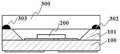
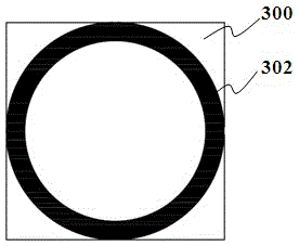
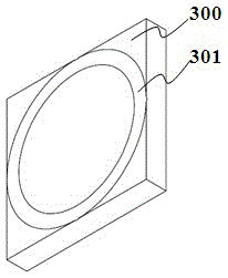
[0036] Such as Figure 1~3 As shown, the present embodiment provides a packaging structure for ultraviolet light emitting diodes, including: a bracket 100, a flip-chip LED chip 200 and a package cover 300, a circuit is formed on the bracket 100, and the LED chip 200 is fixed on the bracket 100 and connected to the bracket. The circuit is electrically connected, the lower surface of the encapsulation cover 300 is provided with a circular groove structure 301, the inner surface of the groove structure is provided with a reflective layer 303, and an organic adhesive 302 is filled in the groove structure 301; The cover body 300 is disposed on the LED chip 200 and connected to the bracket 100 through an organic adhesive 302 .
[0037] The material of the bracket 100 can be a ceramic bracket or a plastic bracket, and the ceramic bracket is preferred in this embodiment. The shape of the bracket preferably has a bowl cup 101 surrounding the LED chip 200 , the groove structure 301 is ...
Embodiment 2
[0048] Such as Figure 4 and 5 As shown, the difference between this embodiment and Embodiment 1 is that: the packaging cover 300 of Embodiment 1 adopts a quartz lens, while the packaging cover 300 of this embodiment adopts a glass cover plate; the groove structure 301 of Embodiment 1 is circular , the groove structure 301 of this embodiment is square and located on the outer edge of the glass cover. The design advantage of this structure is that since the position of the groove structure is far away from the ultraviolet LED light source to the greatest extent, it can further avoid the possible aging of the organic adhesive caused by UV radiation and affect the reliability of the device.
PUM
 Abstract
Description
Claims
Application Information