Formation method of semiconductor structure

A technology of semiconductor and plasma, which is applied in the direction of semiconductor devices, semiconductor/solid-state device manufacturing, electrical components, etc., can solve the problems of semiconductor technology process node shrinkage, the inability to ensure that the structure size formed by etching meets the process requirements, etc., and achieve stable performance, The effect of precise structural dimensions

Active Publication Date: 2020-03-10
SEMICON MFG INT (SHANGHAI) CORP
View PDF4 Cites 0 Cited by
  • Summary
  • Abstract
  • Description
  • Claims
  • Application Information

AI Technical Summary

Problems solved by technology

[0004] However, as the process node of semiconductor technology further shrinks, even if the enhanced patterned mask is used, the structure size formed by etching cannot be guaranteed to meet the process requirements, so further optimization of the process of forming the mask layer is required

Method used


Image

  • Formation method of semiconductor structure
  • Formation method of semiconductor structure
  • Formation method of semiconductor structure

Examples


Embodiment Construction

[0033] As mentioned in the background art, with the reduction of process nodes, the enhanced patterned mask cannot meet the manufacturing process requirements of small-scale structures.

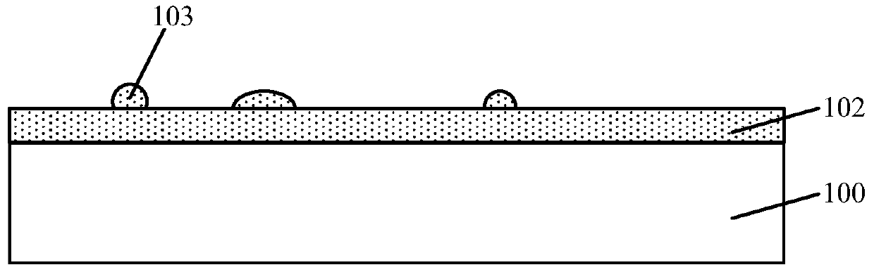
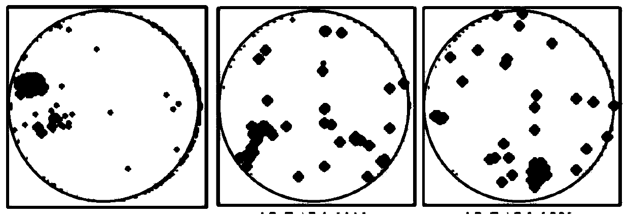
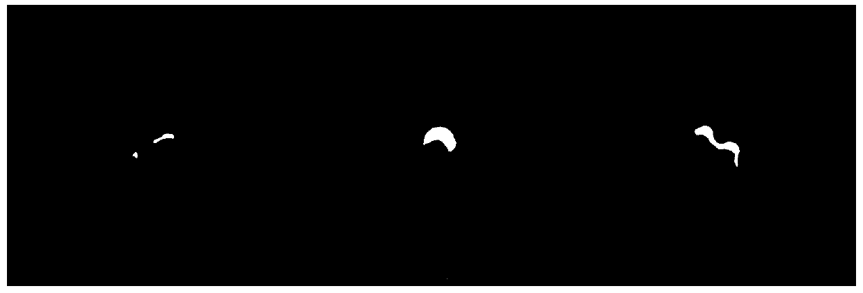
[0034] After research, please refer to figure 1 , figure 1 It is a schematic cross-sectional structure diagram of an embodiment of a semiconductor structure, including: a substrate to be processed 100; an enhanced patterning mask 102 located on the surface of the substrate to be processed 100. The material of the enhanced patterning mask 102 is amorphous carbon (amorphous carbon), and the formation process is plasma enhanced chemical vapor deposition (Plasma Enhanced Chemical Vapor Deposition, PECVD for short). However, since microspheres 103 are likely to be formed on the surface of the formed enhanced patterned mask 102, the microspheres 103 will cause the structural size of the enhanced patterned mask 102 to be inaccurate, and then easily cause the substrate 100 to be processed to be etch...


PUM

PropertyMeasurementUnit
thicknessaaaaaaaaaa
sizeaaaaaaaaaa
thicknessaaaaaaaaaa

Abstract

The invention relates to a formation method of a semiconductor structure. The method comprises that a substrate is provided; a layer to be processed is formed at the surface of the substrate; the surface of the layer to be processed is passivated to reduce the surface activity of the layer to be processed; and a mask layer is formed at the surface of the layer to be processed after passivation. The appearance of the formed semiconductor structure is improved, and the performance stability of the semiconductor structure is improved.

Description

technical field [0001] The invention relates to the technical field of semiconductor manufacturing, in particular to a method for forming a semiconductor structure. Background technique [0002] With the continuous progress of semiconductor technology, the process node of semiconductor technology is continuously reduced, so that the existing mask patterning process and photolithography process are challenged. In order to improve the pattern stability of the mask layer in the photolithography and etching process, an Advance Patterning Film (APF for short) was developed and has received extensive attention in the industry. [0003] The enhanced pattern mask is suitable for the etching process of small-scale patterns. The enhanced patterned mask has the following advantages: First, the enhanced patterned mask has high etching selectivity, since amorphous carbon has a higher etching selectivity compared to various materials, it can only A layer of enhanced patterned mask is us...

Claims


Application Information

Patent Timeline
Patent Type & Authority Patents(China)
IPC IPC(8): H01L21/28H01L21/336
Inventor 周洁鹏陈志刚
Owner SEMICON MFG INT (SHANGHAI) CORP
Why Eureka
Try Eureka