Flat grid field emission electron source device prepared by full-solution method

A technology of emitting electrons and full solution, which is applied in the manufacture of electrode components, etc., to achieve large-scale industrial production and avoid the problem of unstable emission

Inactive Publication Date: 2016-10-26
FUZHOU UNIV
View PDF4 Cites 1 Cited by
  • Summary
  • Abstract
  • Description
  • Claims
  • Application Information

AI Technical Summary

Problems solved by technology

This method can not only achieve large area, flexibility, transparency and low cost, but also avoid the problem of emission instability caused by the introduction of impurities during the preparation process, and realize large-scale industrial production

Method used


Image

  • Flat grid field emission electron source device prepared by full-solution method
  • Flat grid field emission electron source device prepared by full-solution method
  • Flat grid field emission electron source device prepared by full-solution method

Examples


Embodiment Construction

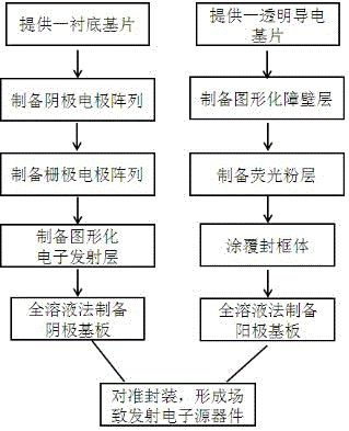
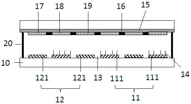
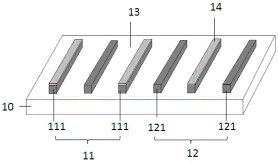
[0046] The present invention will be further described below in conjunction with the accompanying drawings and embodiments. The present invention provides preferred embodiments, but should not be construed as limited to the embodiments set forth herein. In the drawings, the thicknesses of layers and regions are exaggerated for clarity, but should not be considered as strictly reflecting the proportional relationship of geometric dimensions as a schematic diagram.

[0047] The drawings referenced herein are schematic illustrations of idealized embodiments of the invention, and the illustrated embodiments of the invention should not be considered limited to the particular shapes of the regions shown in the drawings, but include resulting shapes, such as manufacturing-induced deviation. All are represented by rectangles in this embodiment, and the representation in the figure is schematic, but this should not be considered as limiting the scope of the present invention.

[0048...


PUM


Abstract

The invention relates to a flat grid field emission electron source device prepared by a full-solution method. A cathode substrate and an anode substrate of a flat grid field emission electron source are prepared by using the full-solution method, and the anode substrate and the cathode substrate are aligned and sealed to form the flat grid field emission electron source device. The cathode substrate comprises a substrate base plate, a cathode electrode array and a grid electrode array arranged on the substrate base plate, and an electron emission layer; the anode substrate comprises a transparent conductive base plate, graphical barrier layers arranged on the transparent base plate, a fluorescent powder layer arranged in the adjacent barrier layers, and a sealing frame arranged around the transparent conductive base plate, and the centers of the adjacent graphical barrier layers and the centers of the corresponding cathode substrates are in one-to-one correspondence. According to the flat grid field emission electron source device prepared by the full-solution method of the invention, large area, flexibility, transparency and low cost can be achieved, the problem of unstable emission caused by introduction of impurities during a preparation process can also be avoided, and the large-scale industrial production can be achieved.

Description

technical field [0001] The invention relates to the field of field emission electron sources, in particular to an all-solution method for preparing flat gate field emission electron source devices. Background technique [0002] Field emission allows electrons to escape from the surface of the emitter without the need for external energy. In vacuum electronic devices, field electron emitters can be used as electron emission sources. The main working principle is to suppress the potential barrier on the surface of the object by a strong external electric field, so that the height of the potential barrier is reduced and the width is narrowed. When the potential barrier When the width is narrow enough to be comparable to the wavelength of electrons, electrons penetrate the potential barrier through the tunnel effect and escape into the vacuum to bombard the anode phosphor to emit light. The electrons emitted by the emission source carry a lot of information about the interior a...

Claims


Application Information

Patent Timeline
Patent Type & Authority Applications(China)
IPC IPC(8): H01J9/18
CPCH01J9/18
Inventor 张永爱孙磊郭太良周雄图林志贤叶芸何林昌靳涛
Owner FUZHOU UNIV
Why Eureka
Try Eureka