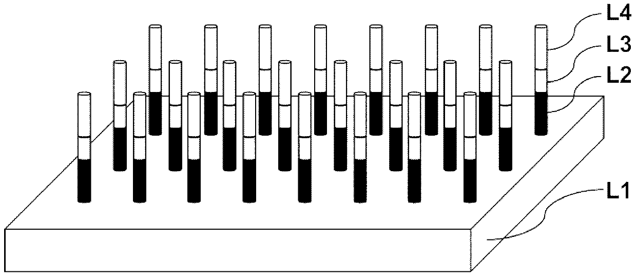
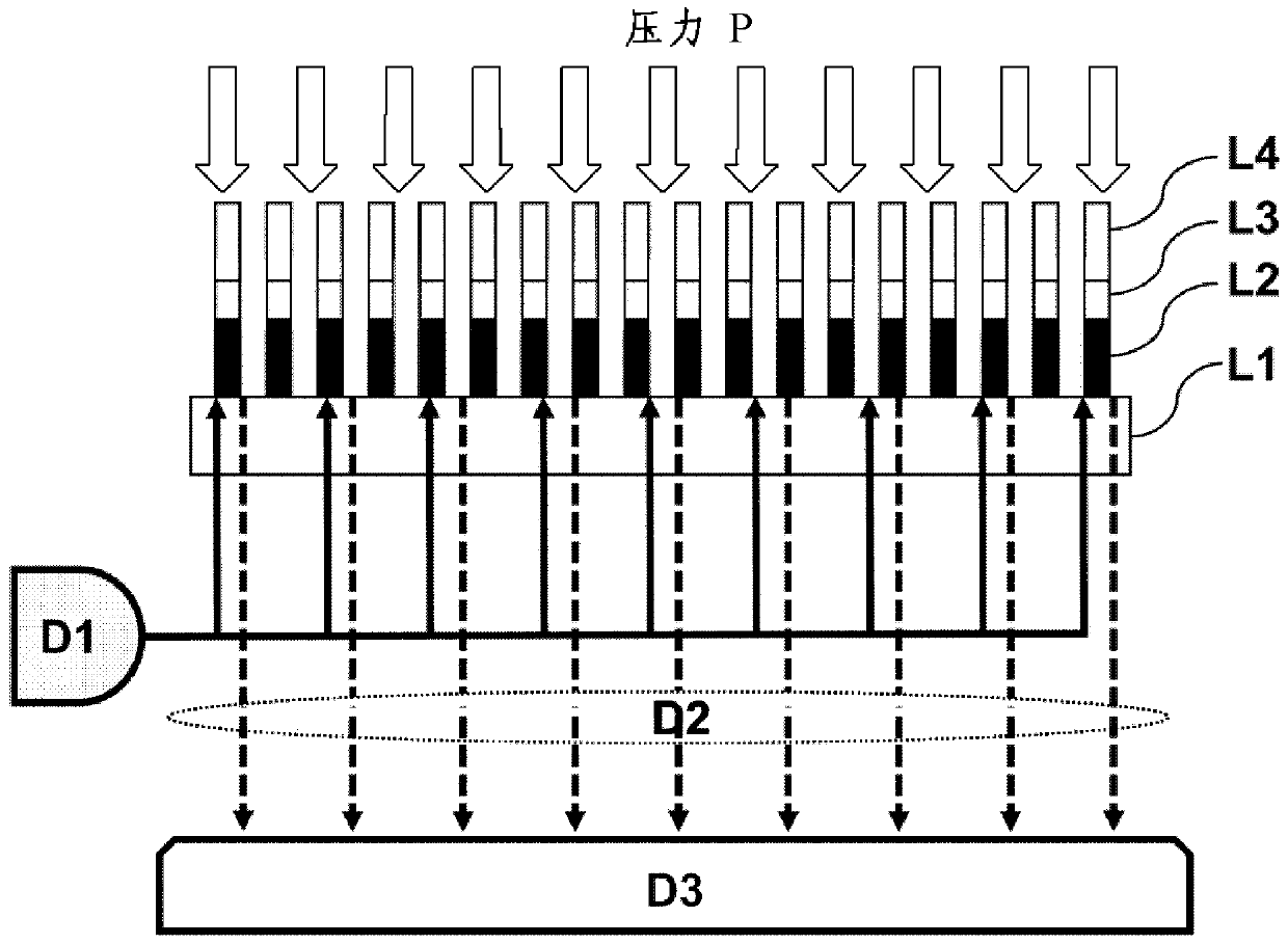
Pressure sensing imaging array, device and method of making the same
An imaging array and sensing technology, applied in the measurement of the property force of piezoelectric devices, and the measurement of force by measuring the change of optical properties of materials when they are stressed, can solve the problem of large number of pixels, complex electrode layout, device Problems such as large self-heating, to achieve the effect of simplifying device processing steps, improving stability and reliability, and reducing manufacturing costs
- Summary
- Abstract
- Description
- Claims
- Application Information
AI Technical Summary
Problems solved by technology
Method used
Image
Examples
Embodiment 1
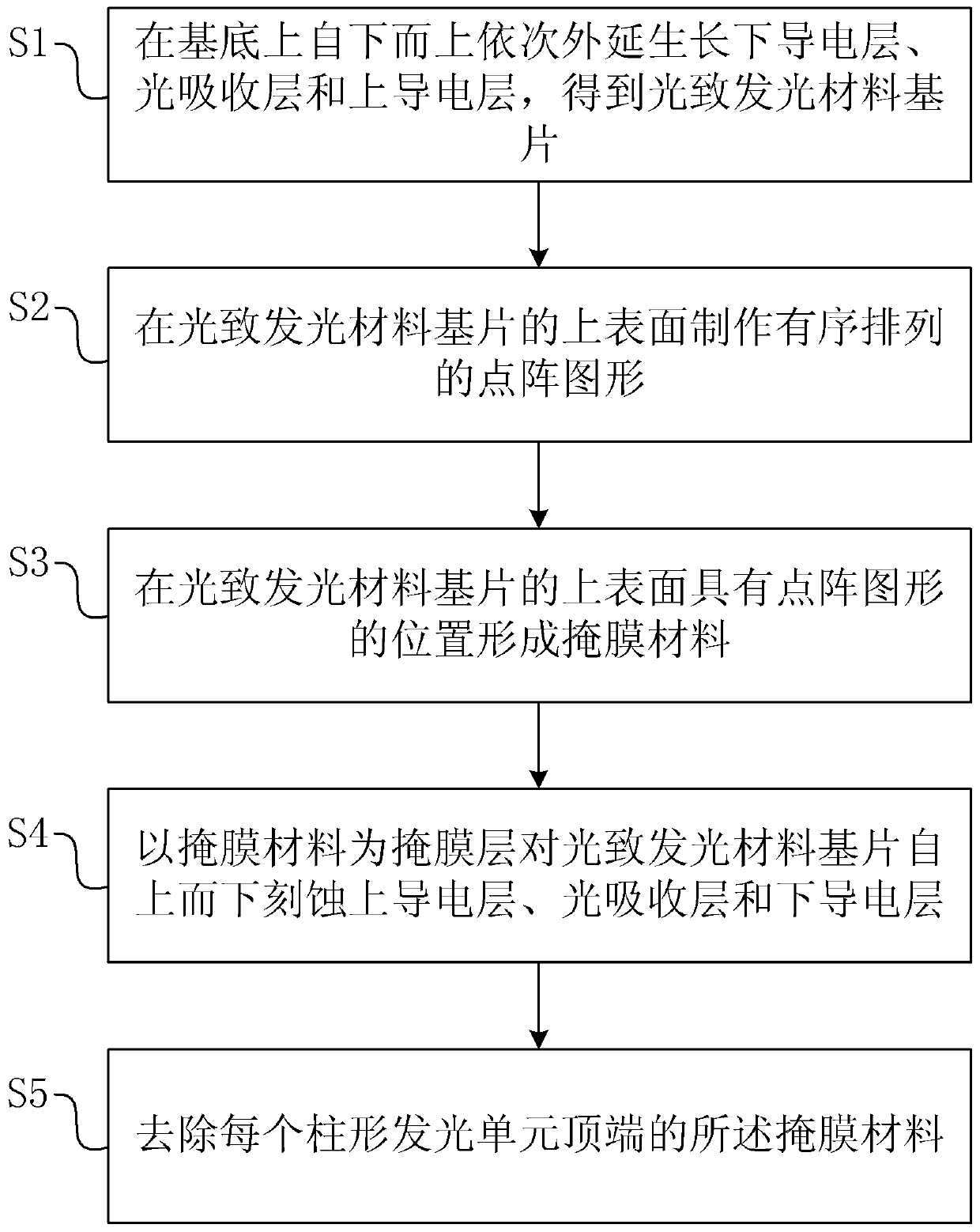
[0068] This embodiment is a multi-quantum well type pressure sensing imaging array and a manufacturing method thereof. Follow the steps below in sequence:
[0069] S1. On the double-polished (0001) surface sapphire substrate, the n-type GaN conductive layer and 5 In 0.18 Ga 0.82 The N / GaN quantum well light absorption layer and the p-type GaN conductive layer are prepared to obtain a GaN-based photoinduced blue light material substrate.
[0070] S2. Using ultraviolet lithography means to make a dot matrix pattern on the GaN-based photo-induced blue light material substrate, the density of which is 1×10 5 mm -2 .
[0071] S3. Depositing a Ni metal thin film on the GaN-based photoluminescent blue light material substrate with a lattice pattern, and then performing a metal lift-off treatment to obtain a large-area and ordered Ni metal lattice array.
[0072] S4. Using the Ni metal lattice array as a mask layer, perform top-down dry etching on the GaN-based photoluminescent m...
Embodiment 2
[0077] This embodiment is a heterojunction pressure sensing imaging array and a manufacturing method thereof. Follow the steps below in sequence:
[0078] S1. Sequential epitaxial growth of n-type Al on double-polished (0001) sapphire substrates 0.6 Ga 0.4 N conductive layer, GaN light absorbing layer and p-type Al 0.1 Ga 0.9 An N conductive layer is prepared to obtain a GaN-based photoinduced ultraviolet light material substrate.
[0079] S2. Using ultraviolet lithography means to make dot matrix patterns on the GaN-based photoinduced ultraviolet material substrate, the density of which is 1×10 3mm -2 .
[0080] S3. Depositing a Ni metal thin film on the GaN-based photo-ultraviolet material substrate with a lattice pattern, and then performing a metal lift-off treatment to obtain a large-area and ordered Ni metal lattice array.
[0081] S4. Using the Ni metal lattice array as a mask layer, dry-etch the GaN-based photo-ultraviolet material substrate from top to bottom, ...
PUM
| Property | Measurement | Unit |
|---|---|---|
| thickness | aaaaa | aaaaa |
Abstract
Description
Claims
Application Information


