Transparent conductive film

A technology of transparent conductivity and transparent conductive layer, which is applied in the direction of conductive layer, metal/alloy conductor, electrical digital data processing, etc. Speed ​​and other issues

Active Publication Date: 2016-10-26
NITTO DENKO CORP
View PDF7 Cites 2 Cited by
  • Summary
  • Abstract
  • Description
  • Claims
  • Application Information

AI Technical Summary

Problems solved by technology

Conventionally, a transparent conductive film having a dry optical adjustment layer with high scratch resistance and an appropriate etching rate of the transparent conductive layer has not been known

Method used


Image

  • Transparent conductive film
  • Transparent conductive film
  • Transparent conductive film

Examples


Embodiment 1

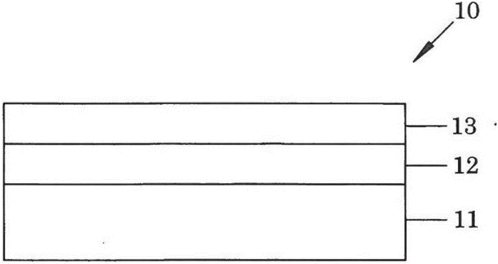
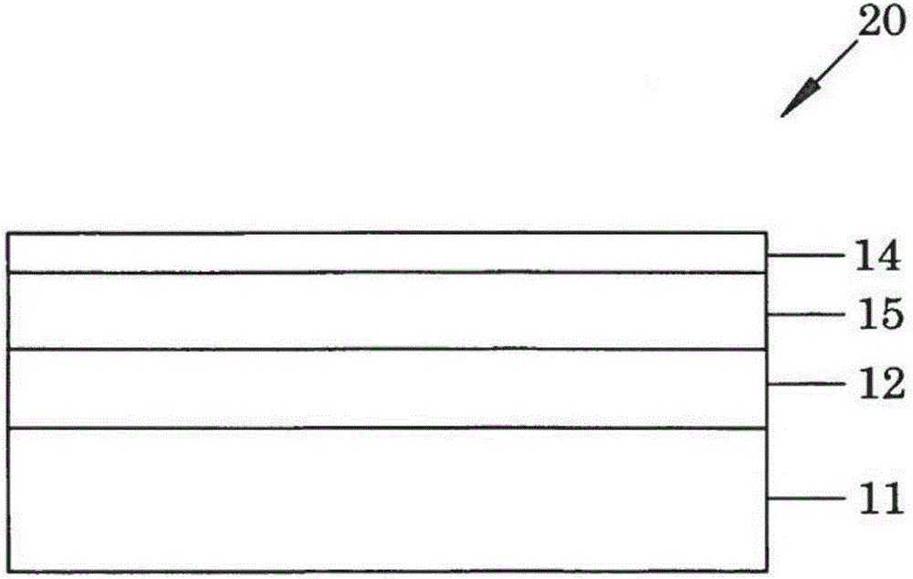
[0091] The transparent conductive film of Example 1 is figure 2 The layer structure shown in . The film substrate is a polyethylene terephthalate (PET) film with a thickness of 100 μm. The optical adjustment layer was composed of a silicon oxide layer formed by sputtering, and had a thickness of 20 nm. The first transparent conductive thin layer was composed of a first indium tin oxide (ITO) layer (thickness 3 nm), and the second transparent conductive thin layer was composed of a second indium tin oxide (ITO) layer (thickness 19 nm). The content ratio of tin (impurity metal element) to indium in the first indium tin oxide layer (first transparent conductive thin layer) (the atomic ratio Sn / In of the number of Sn atoms to the number of In atoms) was 0.03, and the first The content ratio of tin (impurity metal element) to indium in the indium tin oxide layer (second transparent conductive thin layer) (the atomic ratio Sn / In of the number of Sn atoms to the number of In atoms...

Embodiment 2

[0103] Except that the thickness of the first indium tin oxide layer (first transparent conductive thin layer) was 6 nm, and the thickness of the second indium tin oxide layer (second transparent conductive thin layer) was 16 nm, In the same manner as in Example 1, the transparent conductive film of Example 2 was produced.

Embodiment 3

[0105] Except that the thickness of the first indium tin oxide layer (first transparent conductive thin layer) was 8 nm, and the thickness of the second indium tin oxide layer (second transparent conductive thin layer) was 14 nm, In the same manner as in Example 1, the transparent conductive film of Example 3 was produced.


PUM

PropertyMeasurementUnit
thicknessaaaaaaaaaa
densityaaaaaaaaaa
surface roughnessaaaaaaaaaa

Abstract

The invention achieves a transparent conductive film which comprises a dry optical adjustment layer in order to increase scratch resistance, and still has an adequate etching rate of a transparent conductive layer. A transparent conductive film (10) which is obtained by sequentially laminating an optical adjustment layer (12) and a transparent conductive layer (13) in this order on a main surface of a transparent film base (11). The optical adjustment layer (12) comprises a dry optical adjustment layer that contains an inorganic oxide. The transparent conductive layer (13) contains a metal oxide that contains indium. The transparent conductive layer (13) is crystalline, and has at least X-ray diffraction peaks corresponding to the (400) plane and the (440) plane; and if I400 is the X-ray diffraction peak intensity of the (400) plane and I440 is the X-ray diffraction peak intensity of the (440) plane, the X-ray diffraction peak intensity ratio I440 / I400 is within the range of 1.0-2.2.

Description

technical field [0001] The present invention relates to a transparent conductive film. Background technique [0002] Conventionally, a transparent conductive film in which a transparent conductive layer is laminated on one main surface of a transparent film substrate has been known. Transparent conductive films are widely used in devices such as touch panels. When a transparent conductive film is used in a touch panel or the like, for example, a fine wiring pattern is formed on the transparent conductive layer by photolithography, and after development, wet etching is performed to form a fine wiring pattern. At this time, if the etching rate of the transparent conductive layer is too high, for example, the wiring pattern cannot be formed with high accuracy due to problems such as side etching of the fine wiring. On the contrary, if the etching rate of the transparent conductive layer is too slow, the productivity of the patterning process will decrease. In this way, there...

Claims


Application Information

Patent Timeline
Patent Type & Authority Applications(China)
IPC IPC(8): H01B5/14B32B7/02G06F3/041C23C14/08
CPCC23C14/086C23C14/10C23C14/35G06F3/041H01B1/02H01B5/14C23C14/081C23C14/34
Inventor 藤野望加藤大贵梨木智刚
Owner NITTO DENKO CORP
Why Eureka
Try Eureka