A kind of 3D global pixel structure and preparation method thereof

A global pixel and 3D technology, applied in image communication, electrical components, radiation control devices, etc., can solve the problems of high manufacturing difficulty, complex structure, increased pixel readout noise, etc., to reduce chip area and improve optical channel, improving the effect of optical isolation

CN106067467BActive Publication Date: 2018-12-18SHANGHAI INTEGRATED CIRCUIT RES & DEV CENT +1
4 Cites 0 Cited by

Patent Information

Authority / Receiving Office
CN · China
Patent Type
Patents(China)
Current Assignee / Owner
Publication Date
2018-12-18

Smart Images

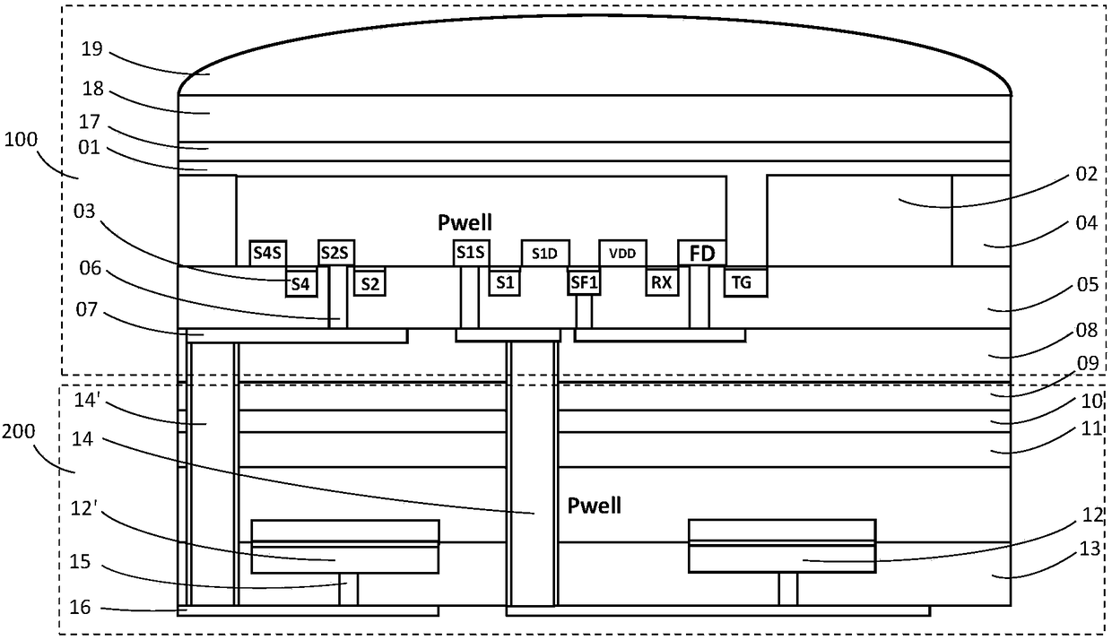
  • Figure 1
    Figure 1
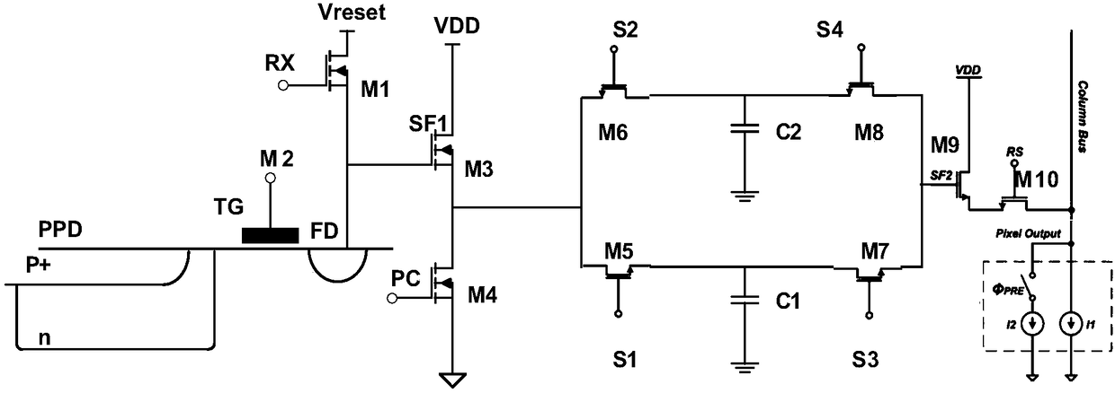
  • Figure 2
    Figure 2
  • Figure 3
    Figure 3
Patent Text Reader

Abstract

The invention discloses a 3D global pixel structure and a preparation method thereof, comprising a photoelectric signal generating circuit unit fabricated on a first silicon substrate layer, a signal storage capacitor unit fabricated on a second silicon substrate layer, and a photoelectric signal generating circuit The unit and the signal storage capacitor unit are arranged in the vertical direction, and the interconnection between the photoelectric signal generation circuit unit and the signal storage capacitor unit is realized through the connection between the through hole, the metal wiring and the contact hole; the present invention adopts the back According to the technology and 3D stacking structure, the three-dimensional unit structure is made at different levels, which can realize the vertical interconnection of the photoelectric signal generation circuit unit and the signal storage capacitor unit, which not only improves the optical path between the outside world and the photodiode, but also improves the signal storage. The optical isolation of the capacitor is improved, and the chip area occupied by the pixel unit is reduced.
Need to check novelty before this filing date? Find Prior Art

Description

technical field

[0001] The invention relates to the technical field of semiconductor image sensing, and more particularly, to a high fill factor global shutter pixel unit with a 3D structure and a preparation method thereof. Background technique

[0002] Traditional global shutter pixel technology is mainly used in CCD image sensors. Due to the increasing popularity of CMOS image sensors, and because machine vision, film production, industrial, automotive, and scanning applications must capture fast-moving objects with high Traditional barriers associated with shutter pixel technology. With this effort, the provided global shutter pixel technology has smaller pixel size, larger fill factor, lower dark current, and lower noise, making CMOS image sensors the preferred choice for CCD sensors in more applications. Viable alternatives.

[0003] In the traditional global pixel, the photosensitive diode and the signal storage and readout circuit unit devices are all manufactured...

Examples

Embodiment Construction

[0040] In order to make the content of the present invention clearer and easier to understand, the content of the present invention will be further described below in conjunction with the accompanying drawings. Of course, the present invention is not limited to this specific embodiment, and general replacements known to those skilled in the art are also covered within the protection scope of the present invention.

[0041] The 3D global pixel structure of the present invention at least includes a photoelectric signal generating circuit unit fabricated on the first silicon substrate layer and a signal storage capacitor unit fabricated on the second silicon substrate layer; the photoelectric signal generating circuit unit and the signal storage capacitor unit Arranged in the vertical direction, and realize the interconnection between the photoelectric signal generating circuit unit and the signal storage capacitor unit through the connection of through holes, contact holes and me...