In-situ transmission electron microscopy based nanometer material alternating-current electrical property test device and method

An electron microscope, electrical performance technology, applied in the measurement device, material capacitance, material analysis using wave/particle radiation, etc., can solve the problem of lack of alternating current test methods, etc., to achieve intuitive and easy-to-read test results, comprehensive electrical parameter information, Simple to use effects

Active Publication Date: 2016-11-16
SOUTHEAST UNIV
View PDF7 Cites 1 Cited by
  • Summary
  • Abstract
  • Description
  • Claims
  • Application Information

AI Technical Summary

Problems solved by technology

The existing technology is generally a direct current test, lacking a test method for alternating current

Method used


Image

  • In-situ transmission electron microscopy based nanometer material alternating-current electrical property test device and method
  • In-situ transmission electron microscopy based nanometer material alternating-current electrical property test device and method
  • In-situ transmission electron microscopy based nanometer material alternating-current electrical property test device and method

Examples


Embodiment 1

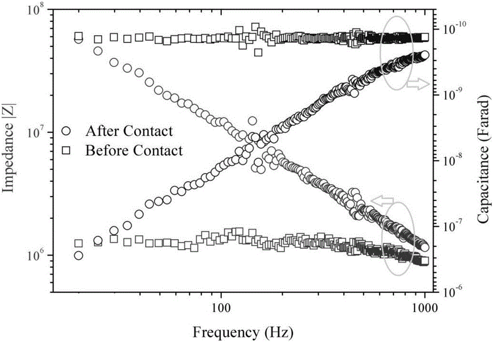
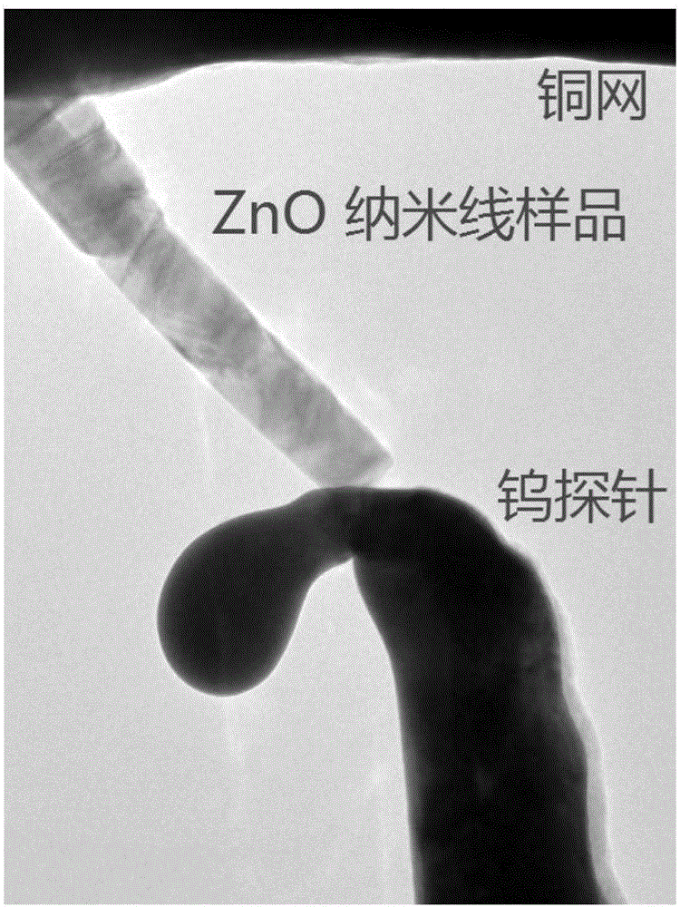
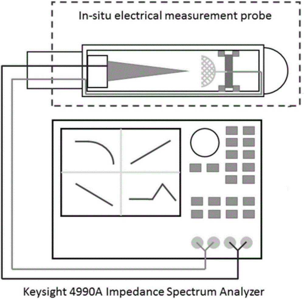
[0025] On the basis of transmission electron microscope (TEM), an AC electrical performance testing device was built, ZnO nanowire samples were prepared, and the samples were loaded into the sample rod fixed on the AC electrical performance testing device, and the nano-manipulator was controlled to suspend the tungsten probe. On the basis of in-situ observation, the electrical parameters of the ZnO nanowire sample were tested in real time by an impedance analyzer to obtain electrical parameters such as impedance and capacitance, and the electrical performance curves before and after the contact between the tungsten probe and the nanowire sample were collected;

[0026] Before the contact between the tungsten probe and the ZnO nanowire, the test characterization method based on the AC electrical properties in the in-situ transmission electron microscope The test results (frequency / impedance / capacitance) are as follows: figure 1 The curve formed by the square in the middle is sho...

Embodiment 2

[0029] On the basis of a transmission electron microscope (TEM), an AC electrical performance test device was built, ZnO nanowire samples were prepared, and the samples were loaded into the device, and the nano-manipulator was controlled to make the tungsten probe contact with the ZnO nanowire samples, and observed in situ On the basis of the ZnO nanowire sample, the impedance analyzer is used to test the electrical parameters of the ZnO nanowire sample in real time, to obtain electrical parameters such as impedance and capacitance, and to collect the electrical performance curves before and after the contact between the tungsten probe and the nanowire sample;

[0030] After the tungsten probe is in contact with the ZnO nanowire, the test characterization method based on the AC electrical performance in the in-situ transmission electron microscope (frequency / impedance / capacitance) is as follows: figure 1 The curve formed by the middle circle is shown;

[0031] In-situ observat...


PUM


Abstract

The invention discloses an in-situ transmission electron microscopy based nanometer material alternating-current electrical property test device. The test device comprises a nanowire sample, an in-situ electrical test device and an impedance spectroscopy analyzing device. The in-situ electrical test device comprises a tungsten tipped probe and a nanowire sample holder; the nanowire sample can be fixed to the nanowire sample holder; the tungsten tipped probe is controlled through a nano micro-manipulation rod to contact with the nanowire sample; after the tungsten tipped probe contacts with the nanowire sample, the tungsten tipped probe, the nanowire sample and the impedance spectroscopy analyzing device form a circuit. After the sample is loaded into the established alternating-current electrical property test device, contact state of the probe and the sample can be changed by application of test alternating-current signals and control of the nano micro-manipulation rod, operations are much simpler than those of other methods, test results are intuitive and have quantitative test characteristics, comprehensive electrical parameter information is achieved, and the test device can be widely applied to electrical property test of various nano materials in the future.

Description

technical field [0001] The invention relates to the field of in-situ detection of nanomaterial properties, in particular to a device and method for testing the alternating current electrical properties of nanomaterials based on an in-situ transmission electron microscope. Background technique [0002] Nanomaterials refer to materials that have at least one dimension in the three-dimensional space in the nanoscale range (1-100nm) or are composed of them as basic units. According to different structures, it can be divided into: three-dimensional, two-dimensional, one-dimensional and zero-dimensional. One-dimensional nanomaterials include nanowires, nanorods and nanoribbons, etc., whose surface effect, quantum size effect, small size effect and macroscopic quantum tunneling effect make them play an important role in nanoelectronic devices. As the cornerstone of nanoelectronic devices, one-dimensional nanomaterials must first have a comprehensive understanding of their electric...

Claims


Application Information

Patent Timeline
Patent Type & Authority Applications(China)
IPC IPC(8): G01N23/22G01N27/02G01N27/22G01N1/28
CPCG01N1/28G01N23/22G01N23/2202G01N23/2206G01N27/02G01N27/22
Inventor 孙立涛马青董辉张秋波徐涛苏适
Owner SOUTHEAST UNIV
Why Eureka
Try Eureka