

Chip packaging structure and packaging method thereof
A chip packaging structure and packaging method technology, which is applied to electrical components, electrical solid-state devices, circuits, etc., can solve problems such as chip wafer warpage, and achieve the effects of low cost, simple process, and warpage reduction.
- Summary
- Abstract
- Description
- Claims
- Application Information
AI Technical Summary
Problems solved by technology
Method used
Image

Examples
Embodiment approach
[0051] As a preferred embodiment, a packaging method of a chip packaging structure in the present invention includes the following steps, see Figure 10 :
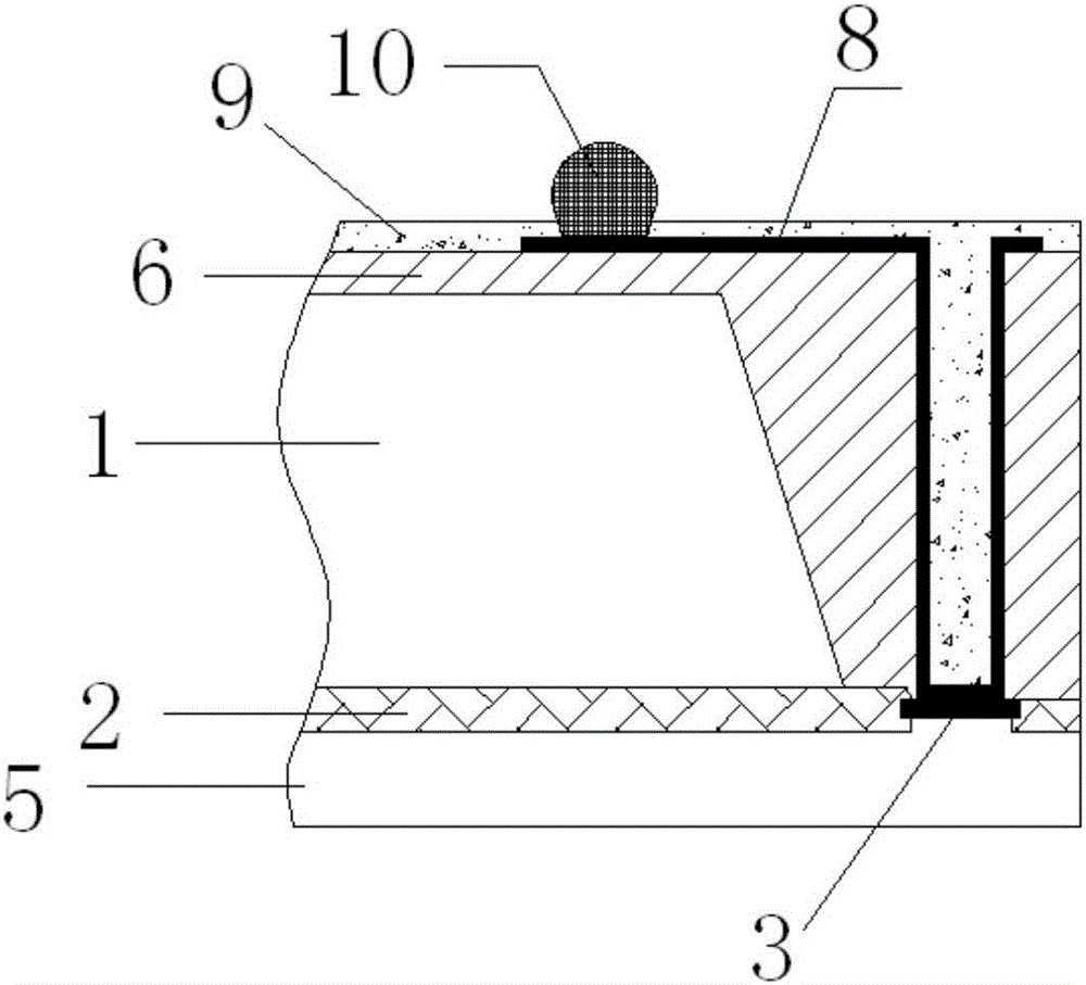
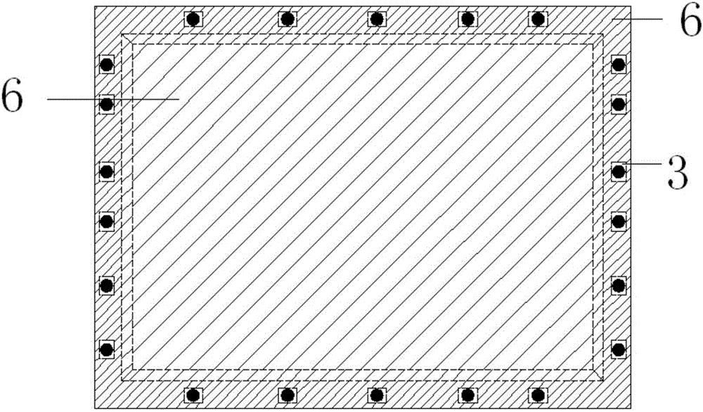
[0052] Step 1, see image 3 , take a wafer including a plurality of chip units 1, wherein the front of the chip unit has a dielectric layer 2, the middle part of the chip unit is a component area, and there are several welding pads 3 in or on the dielectric layer around the chip unit;
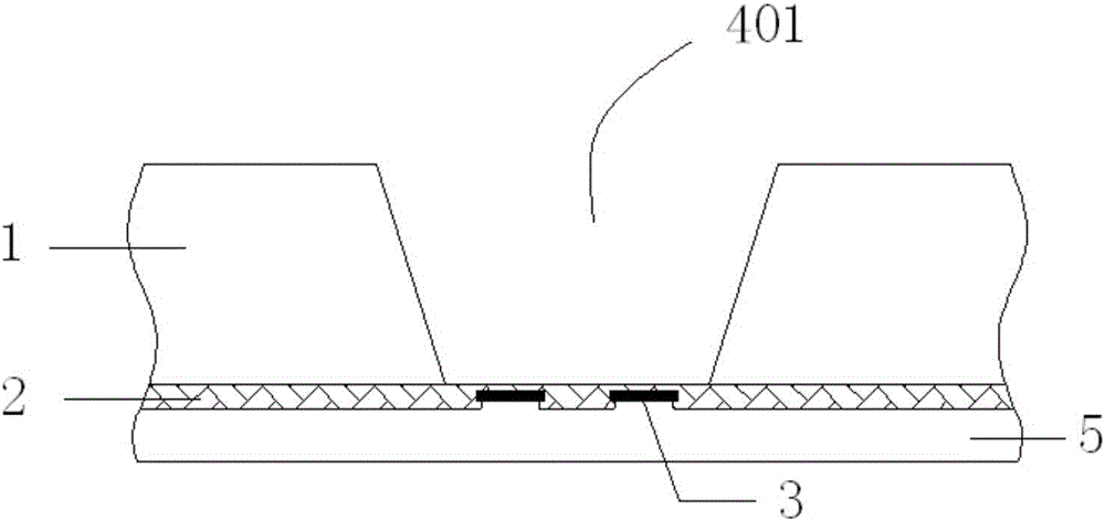
[0053] A pre-opening 401 is formed at a position between adjacent chip units on the back of the wafer, and the pre-opening removes chip substrate material on the pad and exposes the dielectric layer on the back of the pad. The method of forming the pre-opening is dry etching, wet etching or cutting.
[0054] Optionally, before forming the pre-opening, the back of the wafer can be thinned to thin the package thickness of the chip.
[0055] Optionally, before forming the pre-opening, a (temporary) carrier is bonded or not bonded on the fro...
PUM
 Abstract
Description
Claims
Application Information