Thin film transistor, manufacturing method thereof, array substrate and display panel
A technology of thin film transistor and substrate substrate, which is applied in the fields of array substrate, thin film transistor and its manufacturing method, and display panel, can solve the problems of unsatisfactory adjustment effect and small on-current, so as to increase the number and improve the on-current. , the effect of increasing the light intensity
- Summary
- Abstract
- Description
- Claims
- Application Information
AI Technical Summary
Problems solved by technology
Method used
Image

Examples
Embodiment 1
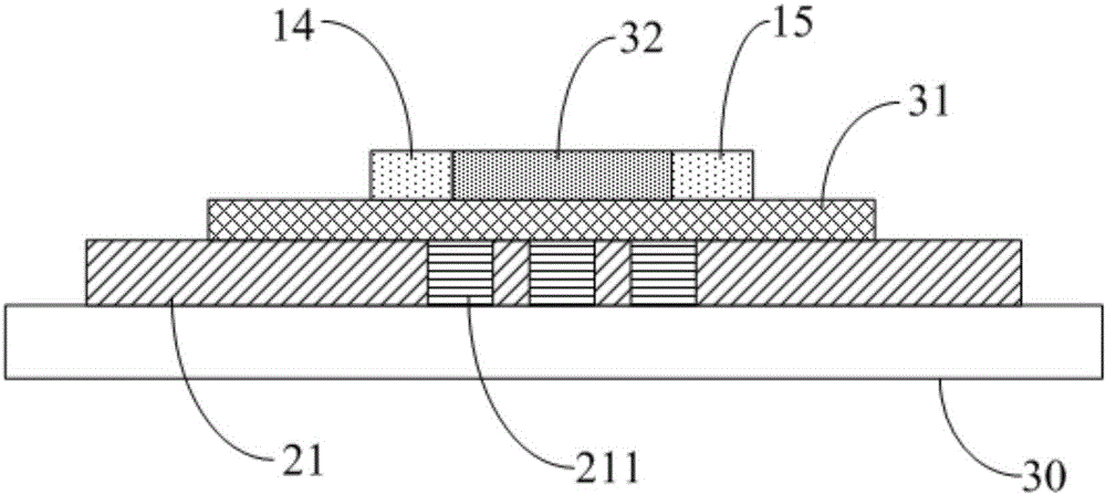
[0041] As shown in FIG. 3( a ), the thin film transistor provided by a specific embodiment of the present invention includes: a base substrate 30 , a gate electrode 21 provided with a plurality of hollow areas on the base substrate 30 , and a transparent conductive material filled in the hollow areas 211 , the electrochromic layer 31 on the transparent conductor 211 , the semiconductor active layer 32 on the electrochromic layer 31 , the source electrode 14 and the drain electrode 15 . The specific arrangements of the semiconductor active layer 32 , the source electrode 14 and the drain electrode 15 of the thin film transistor in the specific embodiment of the present invention are similar to those in the prior art, and are not repeated here.
[0042] The base substrate 30 in the specific embodiment of the present invention is a glass substrate. Of course, in the actual production process, the base substrate 30 may also be other types of substrates such as plastic substrates. ...
Embodiment 2
[0050] As shown in FIG. 3( b ), the thin film transistor provided by the specific embodiment of the present invention includes: a base substrate 30 , a gate electrode 21 provided with a plurality of hollow areas on the base substrate 30 , an electrochromic electrode filled in the hollow areas layer 31, insulating layer 34 on the electrochromic layer 31, semiconductor active layer 32 on the insulating layer 34, source electrode 14 and drain electrode 15, the electrochromic layer 31 in the specific embodiment of the present invention adopts conductivity The insulating layer 34 adopts the commonly used insulating material in the prior art, such as: the insulating layer 34 adopts a single-layer film of silicon oxide or silicon nitride, or a composite film of silicon oxide and silicon nitride. The specific embodiment does not limit the specific material of the insulating layer 34 .
[0051] Specifically, when the thin film transistor in the specific embodiment of the present invent...
PUM
 Abstract
Description
Claims
Application Information
 - R&D
- Intellectual Property
- Life Sciences
- Materials
- Tech Scout
- Unparalleled Data Quality
- Higher Quality Content
- 60% Fewer Hallucinations
Browse by: Latest US Patents, China's latest patents, Technical Efficacy Thesaurus, Application Domain, Technology Topic, Popular Technical Reports.
© 2025 PatSnap. All rights reserved.Legal|Privacy policy|Modern Slavery Act Transparency Statement|Sitemap|About US| Contact US: help@patsnap.com