1064nm enhanced Si-PIN photoelectric detector and manufacturing method thereof
A technology for photodetectors and manufacturing methods, which is applied in the field of photodetectors, can solve the problems of low responsivity at 1064nm wavelength, etc., and achieve the effects of easy product production, easy integration, and small surface damage
- Summary
- Abstract
- Description
- Claims
- Application Information
AI Technical Summary
Problems solved by technology
Method used
Image

Examples
Embodiment Construction
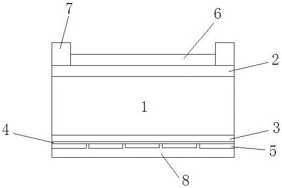
[0027] A 1064nm enhanced Si-PIN photodetector, the innovation of which is: the 1064nm enhanced Si-PIN photodetector consists of an N-type substrate layer 1, a P+ region 2, a black silicon layer 3, an N+ region 4, and a passivation film 5. Anti-reflection film 6, P electrode 7 and N electrode 8;
[0028] The P+ region 2 is formed on the front of the N-type substrate layer 1; the black silicon layer 3 is formed on the back of the N-type substrate layer 1; the anti-reflection film 6 covers the surface of the P+ region 2, and the anti-reflection film 6 is provided There is a P electrode hole, and the P electrode 7 is arranged in the P electrode hole and contacts the P+ region 2; the N+ region 4 covers the surface of the black silicon layer 3; the passivation film 5 covers the N+ region 4 surface, and the passivation film An N electrode hole is arranged on the 5, and an N electrode 8 is arranged in the N electrode hole and is in contact with the N+ region 4; the P+ region 2 forms a...
PUM
 Abstract
Description
Claims
Application Information
 - Generate Ideas
- Intellectual Property
- Life Sciences
- Materials
- Tech Scout
- Unparalleled Data Quality
- Higher Quality Content
- 60% Fewer Hallucinations
Browse by: Latest US Patents, China's latest patents, Technical Efficacy Thesaurus, Application Domain, Technology Topic, Popular Technical Reports.
© 2025 PatSnap. All rights reserved.Legal|Privacy policy|Modern Slavery Act Transparency Statement|Sitemap|About US| Contact US: help@patsnap.com