Light-emitting diode and manufacturing method thereof

A technology for light-emitting diodes and a manufacturing method, which is applied to electrical components, circuits, semiconductor devices, etc., can solve problems such as lattice mismatch, threading dislocation defects, and reduced luminous efficiency of light-emitting diode devices, and achieves improved luminous efficiency, small The effect of threading dislocation density

Active Publication Date: 2016-11-16
MIKRO MESA TECH
View PDF5 Cites 7 Cited by
  • Summary
  • Abstract
  • Description
  • Claims
  • Application Information

AI Technical Summary

Problems solved by technology

Since the two materials have different lattice constants and thermal expansion coefficients, the lattice mismatch between the two materials will generate stress during material deposition, resulting in the generation of threading dislocation defects
If threading dislocation defects are generated in the light-emitting region of the LED device, the luminous efficiency of the LED device will be reduced, especially for light-emitting diodes that enter the micron scale.

Method used


Image

  • Light-emitting diode and manufacturing method thereof
  • Light-emitting diode and manufacturing method thereof
  • Light-emitting diode and manufacturing method thereof

Examples


Embodiment Construction

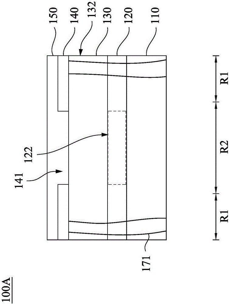
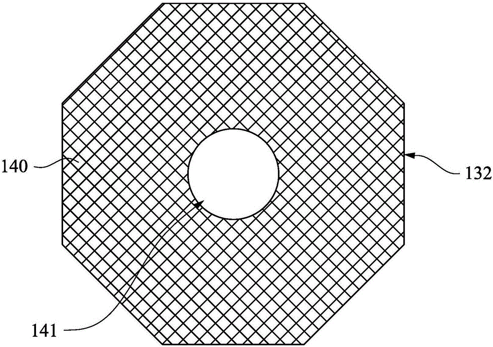
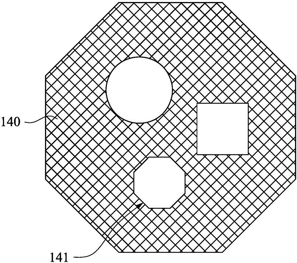
[0022] A number of implementations of the present invention will be disclosed below in conjunction with the accompanying drawings. For the sake of clarity, many practical details will be described together in the following description. It should be understood, however, that these practical details should not be used to limit the invention. That is, in some embodiments of the present invention, these practical details are unnecessary. In addition, for the sake of simplifying the drawings, some well-known and commonly used structures and elements will be shown in a simple and schematic manner in the drawings.

[0023] As used herein, "about", "approximately" or "approximately" generally means that the error or range of the value is within about 20%, preferably within about 10%, and more preferably It is within about five percent. If there is no explicit statement in the text, the numerical values ​​mentioned are regarded as approximate values, that is, the error or range indic...


PUM


Abstract

The invention discloses a light-emitting diode and a manufacturing method thereof. The light-emitting diode (LED) includes a first type semiconductor layer, a second type semiconductor layer, an active layer, a dielectric layer and an electrode. The active layer is disposed between the first type semiconductor layer and the second type semiconductor layer. The active layer has at least one threading dislocation therein. The dielectric layer is disposed on the second type semiconductor layer. The dielectric layer has at least one first opening therein to expose a part of the second type semiconductor layer. The vertical projection of the threading dislocation on the dielectric layer is separated from the first opening. The electrode partially is disposed on the dielectric layer and electrically coupled to the second type semiconductor layer through the first opening. Light-emitting efficiency of the light-emitting diode is improved.

Description

technical field [0001] The invention relates to a light emitting diode and a manufacturing method thereof. Background technique [0002] A light emitting diode (light-emitting diode; LED) is a semiconductor light emitting device capable of converting electric current into light energy. As a light source, light-emitting diodes have the advantages of low energy consumption, long service life, small size, and fast response. Therefore, light-emitting diodes have gradually replaced traditional lighting devices such as incandescent lamps. [0003] Accordingly, light-emitting diodes based on gallium nitride (including indium gallium nitride and aluminum gallium nitride) have become the mainstream in the field of light-emitting diode lighting. However, during epitaxy, the luminous efficiency of GaN-based LEDs may be affected by threading dislocation defects. Threading dislocation defects usually arise when epitaxially growing another crystalline material on one material. Since t...

Claims


Application Information

Patent Timeline
Patent Type & Authority Applications(China)
IPC IPC(8): H01L33/02H01L33/14
CPCH01L33/025H01L33/14
Inventor 陈立宜张佩瑜詹志辉张俊仪林师勤李欣薇
Owner MIKRO MESA TECH
Why Eureka
Try Eureka