OLED display device and manufacturing method therefor

A technology for display devices and manufacturing methods, which is applied in semiconductor/solid-state device manufacturing, electric solid-state devices, semiconductor devices, etc., can solve problems such as organic light-emitting layer damage, and achieve the effects of low production cost, simple preparation process, and simple production process

Active Publication Date: 2016-11-16
SHENZHEN CHINA STAR OPTOELECTRONICS TECH CO LTD
View PDF6 Cites 18 Cited by
  • Summary
  • Abstract
  • Description
  • Claims
  • Application Information

AI Technical Summary

Problems solved by technology

However, when forming the PEDOT:PSS film, the solvent of the PEDOT:PSS solution contains water, which can easily damage the organic light-emitt

Method used


Image

  • OLED display device and manufacturing method therefor
  • OLED display device and manufacturing method therefor
  • OLED display device and manufacturing method therefor

Examples


Embodiment Construction

[0038] In order to further illustrate the technical means adopted by the present invention and its effects, the following describes in detail in conjunction with preferred embodiments of the present invention and accompanying drawings.

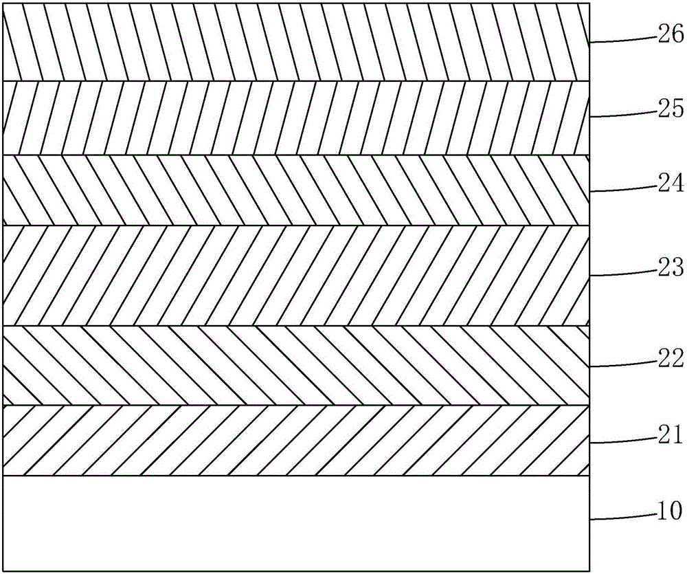
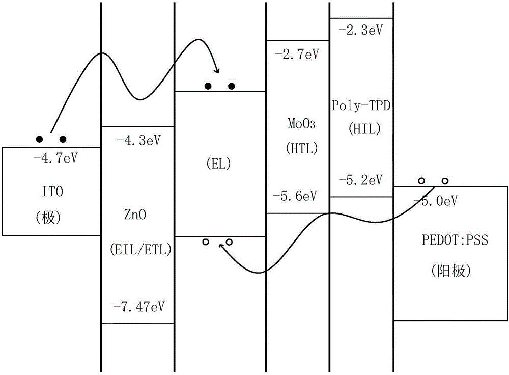
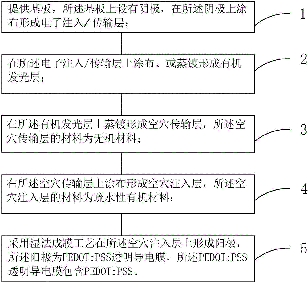
[0039] see figure 1 , is the OLED display device of the present invention, including a substrate 10, a cathode (Cathode) 21 arranged on the substrate 10, an electron injection / transport layer (EIL / ETL) 22 arranged on the cathode 21, and an electron injection / transport layer (EIL / ETL) 22 arranged on the substrate 10. The organic light emitting layer (EL) 23 on the electron injection / transport layer 22, the hole transport layer (HTL) 24 on the organic light emitting layer 23, the hole injection layer on the hole transport layer 24 layer (HIL) 25, and an anode (Anode) 26 disposed on the hole injection layer 25.

[0040] Specifically, the substrate 10 is a TFT array (Array) substrate, and the cathode 21 is a transparent pixel electrode on the TFT...


PUM


Abstract

The invention provides an OLED display device and a manufacturing method therefor. The OLED display device adopts an inverted type device structure and comprises a substrate, a cathode, an electron injection/transporting layer, a hole transporting layer, a hole injection layer and an anode, wherein the anode is a high conductivity PEDOT:PSS transparent conducting film which can be used to form a transparent OLED display device, the hole injection layer is a hydrophobic organic material, the hole transporting layer is an inorganic material which is high in water and oxygen barrier property, and therefore the hydrophobic hole injection layer can effectively prevent water molecules from permeating an organic illuminant layer when the PEDOT:PSS transparent conducting film is made into the anode; the hole transporting layer which is high in water and oxygen barrier property can exert secondary barrier effects on oxygen molecules and water molecules, and an aim of providing dual protection for the organic illuminant layer can be attained; the OLED display device and the manufacturing method therefor have a great batch production advantage due to simple manufacturing technologies and low production cost.

Description

technical field [0001] The invention relates to the technical field of photoelectric display, in particular to an OLED display device and a manufacturing method thereof. Background technique [0002] Organic Light Emitting Diodes (OLED) display devices have self-illumination, low driving voltage, high luminous efficiency, short response time, high definition and contrast, nearly 180° viewing angle, wide operating temperature range, and flexible display With many advantages such as large-area full-color display, it is recognized by the industry as a display device with the most development potential. [0003] OLED display devices belong to self-luminous display devices, and generally include pixel electrodes and common electrodes used as anodes and cathodes respectively, and an organic functional layer arranged between the pixel electrodes and the common electrodes, so that when an appropriate voltage is applied to When the anode and cathode are connected, light is emitted f...

Claims


Application Information

Patent Timeline
IPC IPC(8): H01L51/50H01L51/52H01L51/56
CPCH10K71/12H10K71/166H10K50/17H10K50/805
Inventor 徐超
Owner SHENZHEN CHINA STAR OPTOELECTRONICS TECH CO LTD
Why Eureka
Try Eureka