
Method of manufacturing liquid crystal display panel

A technology for a liquid crystal display panel and a manufacturing method, which is applied in nonlinear optics, instruments, optics, etc., can solve the problems of high cost, reduced product yield, and cannot guarantee the surface flatness of glass substrates, and achieves high strength and avoids damage. Effect

Inactive Publication Date: 2016-11-23
HONG FU JIN PRECISION IND (SHENZHEN) CO LTD +1
View PDF8 Cites 8 Cited by
  • Summary
  • Abstract
  • Description
  • Claims
  • Application Information

AI Technical Summary

Problems solved by technology

Since hydrofluoric acid is an irritating liquid, it is easy to affect the environment
At the same time, the flatness of the surface of the glass substrate cannot be guaranteed during the processing process, which reduces the yield of the product and the cost is high

Method used


Image

  • Method of manufacturing liquid crystal display panel
  • Method of manufacturing liquid crystal display panel
  • Method of manufacturing liquid crystal display panel

Examples


Embodiment Construction

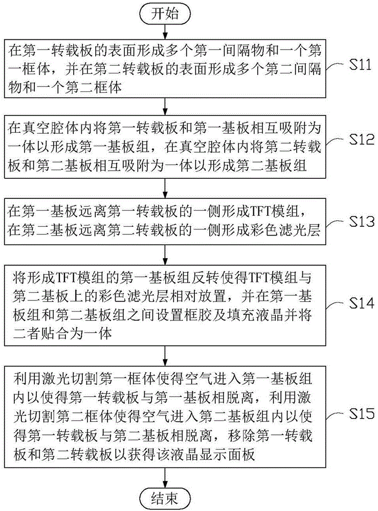
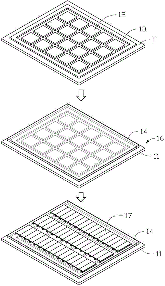
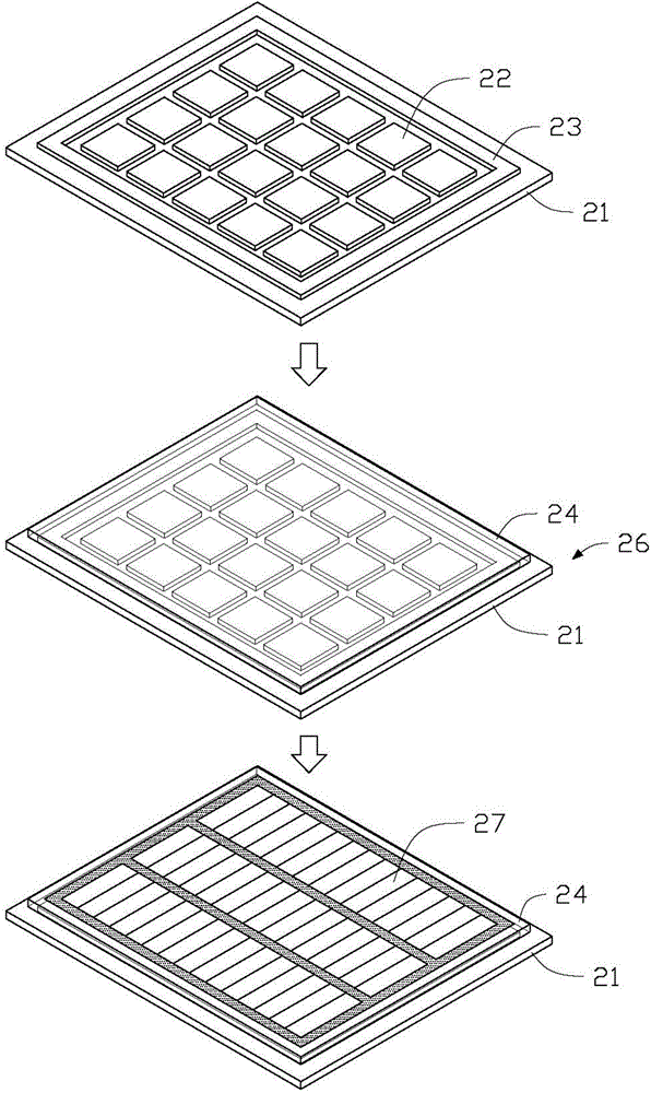
[0022] Please also refer to Figure 1 to Figure 5 , which is a flow chart of a method for manufacturing the liquid crystal display panel 10 in a preferred embodiment. Figure 2-Figure 4 for figure 1 The structure diagram corresponding to each process step shown, Figure 5 for Figure 4 A cross-sectional view of the first substrate group 16 and the second substrate group 26 along the V-V direction. In this embodiment, the liquid crystal display panel 10 is a thin film transistor (TFT-LCD) panel. In other alternative embodiments, the liquid crystal display panel 10 can also be an active matrix organic light emitting diode (AMOLED) panel.

[0023] Step S11 , forming a plurality of first spacers 12 and a first frame body 13 on the surface of the first transfer plate 11 , and forming a plurality of second spacers 22 and a second frame body on the surface of the second transfer plate 21 twenty three. The plurality of first spacers 12 are located in the first frame body 13 and ...


PUM

PropertyMeasurementUnit
thicknessaaaaaaaaaa
thicknessaaaaaaaaaa

Abstract

A method of manufacturing a liquid crystal display panel comprises: forming multiple spacers and a frame respectively on the surfaces of a first transfer board and a second transfer board; in a vacuum chamber, adsorbing the first transfer board and a first substrate to integrally form a first substrate assembly, and adsorbing the second transfer board and a second substrate to integrally form a second substrate assembly; forming a thin-film transistor array on the first substrate and a color filter layer on the second substrate; reversing the first substrate assembly so that the TFT array and the color filter layer are arranged oppositely, and providing frame glue and filling liquid crystal between the first substrate and the second substrate, and attaching them into a whole; laser-cutting a first frame to separate the first transfer board and the first substrate, cutting a second frame to separate the first transfer board and the second substrate, and removing the first transfer board and the second transfer board.

Description

technical field [0001] The present invention relates to a method for manufacturing a liquid crystal display panel. Background technique [0002] In the manufacturing process of the existing liquid crystal display panel, liquid crystal molecules are poured on the glass substrate forming the TFT array and between the glass substrate with the color filter layer to form the liquid crystal display panel. However, in order to meet the user's demand for thinner and lighter products, how to make the liquid crystal display device thinner and lighter is still one of the important topics of current research in the industry. [0003] In the prior art, a chemical reaction between hydrofluoric acid (HF) and glass is used to reduce the thickness of the glass substrate, so as to realize the thinning of the glass substrate. As hydrofluoric acid is an irritating liquid, it is easy to have an impact on the environment. At the same time, the flatness of the surface of the glass substrate cann...

Claims


Application Information

Patent Timeline
Patent Type & Authority Applications(China)
IPC IPC(8): G02F1/1333G02F1/1339
Inventor 陈志芳
Owner HONG FU JIN PRECISION IND (SHENZHEN) CO LTD
Learn More