Inter-chip interconnection structure, manufacturing method of inter-chip interconnection structure and packaging structure

An interconnection structure and packaging structure technology, applied in the semiconductor field, can solve the problems of reducing interconnection pitch, damage to electronic devices, damage to sensitive devices, etc.

Inactive Publication Date: 2016-11-23
TSINGHUA UNIV
View PDF5 Cites 5 Cited by
  • Summary
  • Abstract
  • Description
  • Claims
  • Application Information

AI Technical Summary

Problems solved by technology

The first two technologies have a liquid phase in the bonding process, which limits the continued reduction in interconnect pitch
The thermocompression bonding technology requires a higher bonding temperature (300°C and abo

Method used


Image

  • Inter-chip interconnection structure, manufacturing method of inter-chip interconnection structure and packaging structure
  • Inter-chip interconnection structure, manufacturing method of inter-chip interconnection structure and packaging structure
  • Inter-chip interconnection structure, manufacturing method of inter-chip interconnection structure and packaging structure

Examples


Embodiment Construction

[0040] Specific embodiments of the present invention will be described in detail below in conjunction with the accompanying drawings. It should be understood that the specific embodiments described here are only used to illustrate and explain the present invention, and are not intended to limit the present invention.

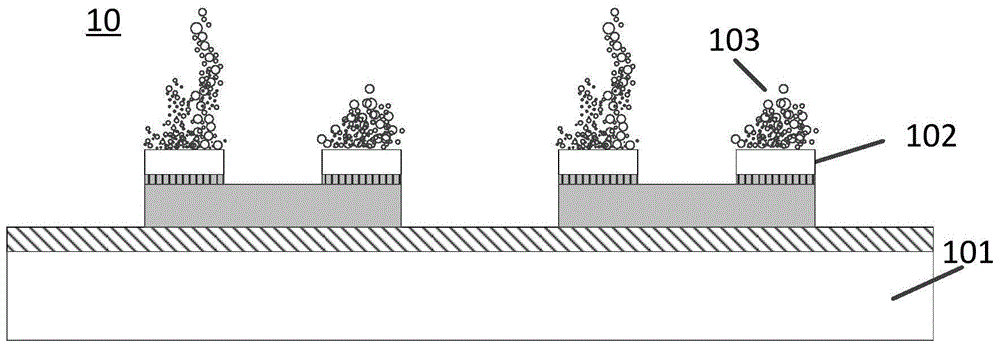
[0041] figure 1 A schematic diagram of an inter-chip interconnect structure 10 according to an embodiment of the present invention is shown. Such as figure 1 As shown, the interchip interconnection structure 10 may include a substrate 101 and first bonding bumps 102 formed on the substrate 101 . The material forming the substrate 101 may include, but not limited to, one of the following: silicon, glass, gallium nitride (GaN), or gallium arsenide (GaAs). The first bonding bump 102 can be any metal suitable for bonding, such as copper (Cu), gold (Au), tin (Sn), aluminum (Al), silver (Ag) and the like. The first bonding bump 102 may be, for example, a film bump...


PUM


Abstract

The invention discloses an inter-chip interconnection structure, a manufacturing method of the inter-chip interconnection structure and a packaging structure. The inter-chip interconnection structure comprises a substrate, and first bonding bumps formed on the substrate, and is characterized by also comprising a first three-dimensional nanostructure which is deposited on the first bonding bumps and has the conductivity. Therefore, continuous reduction of an interlayer pitch can be achieved, the bonding temperature is reduced and the integration level is improved.

Description

technical field [0001] The present invention relates to the field of semiconductors, in particular to an inter-chip interconnection structure, a method for manufacturing the inter-chip interconnection structure and a packaging structure. Background technique [0002] As the function and speed of electronic devices continue to increase, the density of I / O ports of integrated circuits is getting higher and higher, so the pitch (ie, center distance) between pads of electronic components is also shrinking. According to the 2011 report of the International Semiconductor Technology Roadmap (ITRS), it is pointed out that the typical inter-chip interconnect pitch will be reduced to 25 μm in 2015. [0003] Traditional interchip interconnection technologies include solder connection, solid-liquid interdiffusion connection technology, copper-copper (Cu-Cu) thermocompression bonding technology, etc. The first two technologies have a liquid phase in the bonding process, which limits the...

Claims


Application Information

Patent Timeline
IPC IPC(8): H01L23/538H01L21/768B82Y40/00B81B1/00B81C1/00B81C3/00
Inventor 刘子玉蔡坚王谦邹贵生刘磊
Owner TSINGHUA UNIV
Why Eureka
Try Eureka