Silicon carbide junction barrier schottky diode and manufacturing method thereof

The technology of a junction barrier Schottky and its manufacturing method, which is applied in the field of silicon carbide junction barrier Schottky diodes and its manufacture, can solve the problem of low depletion pinch-off ability, improve device reliability, and strengthen vertical The effect of depleting the pinch-off ability

Inactive Publication Date: 2016-11-23
INST OF MICROELECTRONICS CHINESE ACAD OF SCI
View PDF4 Cites 4 Cited by
  • Summary
  • Abstract
  • Description
  • Claims
  • Application Information

AI Technical Summary

Problems solved by technology

And in the reverse depletion, the pinch-off occurs later

Method used


Image

  • Silicon carbide junction barrier schottky diode and manufacturing method thereof
  • Silicon carbide junction barrier schottky diode and manufacturing method thereof
  • Silicon carbide junction barrier schottky diode and manufacturing method thereof

Examples


Embodiment Construction

[0024] Certain embodiments of the invention will be described more fully hereinafter with reference to the accompanying drawings, in which some, but not all embodiments are shown. Indeed, various embodiments of the invention may be embodied in many different forms and should not be construed as limited to these set forth embodiments; rather, these embodiments are provided so that this invention will satisfy applicable legal requirements.

[0025] In order to make the object, technical solution and advantages of the present invention clearer, the present invention will be described in further detail below in conjunction with specific embodiments and with reference to the accompanying drawings.

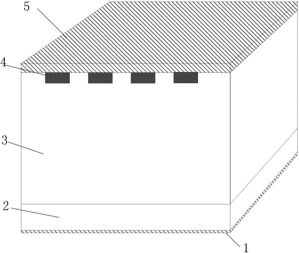
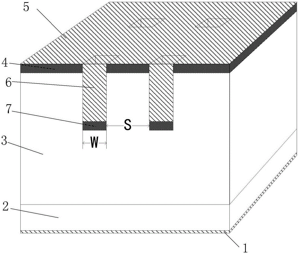
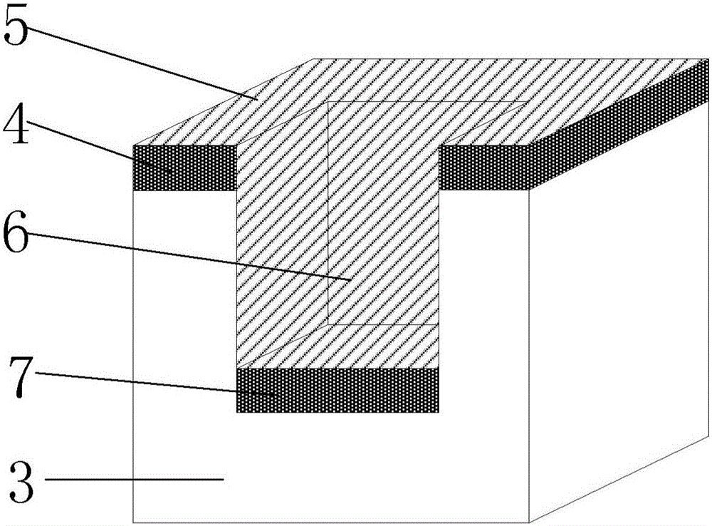
[0026] An embodiment of the present invention provides a silicon carbide junction barrier Schottky diode, such as figure 2 and 3 As shown, it includes: a silicon carbide N-type substrate 2 with a high doping concentration, a cathode electrode 1 is provided on the lower surface of the ...


PUM


Abstract

A silicon carbide junction barrier Schottky diode, comprising: a silicon carbide N-type substrate; a silicon carbide N-type drift region, and a silicon carbide P-type layer, which are sequentially stacked on the upper surface of the silicon carbide N-type substrate; A plurality of grooves are vertically opened downward on the top of the silicon carbide P-type layer, and the depth d of the grooves satisfies d 2 <d<d 1 +d 2 , where d 1 is the thickness of the SiC N-type drift region, d 2 is the thickness of the silicon carbide P-type layer; the P+ injection layer is arranged at the bottom of the plurality of grooves; and the anode electrode is formed at least on the sidewalls of the plurality of grooves, and the silicon carbide junction barrier The special base diode takes advantage of the area of ​​the side wall to increase the current conduction area, increase the conduction current, save the chip area, and strengthen the pinch-off ability of exhaustion, reduce the leakage current during reverse bias, and improve the reverse bias device reliability.

Description

technical field [0001] The invention relates to the field of semiconductor power devices, in particular to a silicon carbide junction barrier Schottky diode and a manufacturing method thereof. Background technique [0002] With the development of modern technology, people continue to put forward higher requirements for semiconductor power devices in terms of volume, reliability, withstand voltage, and power consumption. Traditional silicon devices are limited [0003] In terms of the characteristics of the material itself, it is getting closer and closer to its theoretical limit, and people urgently need to explore new materials other than silicon materials. Silicon carbide has a series of advantages that traditional silicon materials do not have, such as higher breakdown electric field, higher thermal conductivity, and larger forbidden band width, making silicon carbide more suitable for high-voltage power applications. [0004] The silicon carbide junction barrier contro...

Claims


Application Information

Patent Timeline
IPC IPC(8): H01L29/872H01L21/329H01L29/24
CPCH01L29/872H01L29/24H01L29/6606
Inventor 汤益丹邓小川白云郭飞宋凌云杨成樾
Owner INST OF MICROELECTRONICS CHINESE ACAD OF SCI
Why Eureka
Try Eureka