Nitride light emitting diode
A technology of light-emitting diodes and nitrides, which is applied in the direction of electrical components, circuits, semiconductor devices, etc., and can solve the problems of different reflected light paths, affecting the light-emitting angle and light extraction efficiency, etc.
- Summary
- Abstract
- Description
- Claims
- Application Information
AI Technical Summary
Problems solved by technology
Method used
Image
Examples
Embodiment 1
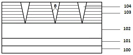
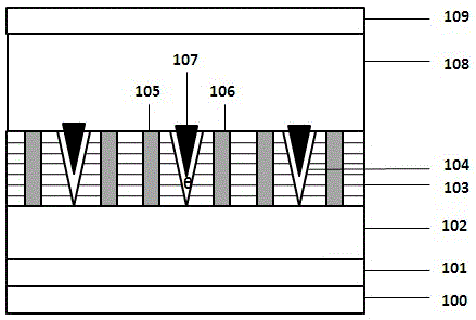
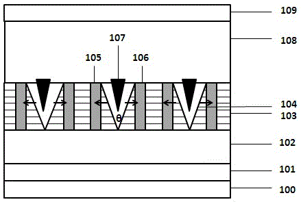
[0020] Tensile stress is applied to both sides of the V-Pits sidewall to make its opening angle larger. First, on the sapphire substrate 100, epitaxially grow the buffer layer 101, N-type nitride 102, multiple quantum wells 103, V-pits 104 due to the extension of dislocations in the multiple quantum wells; then, take out the epitaxial wafer after growing the quantum wells , carry out photolithography and evaporation, and deposit materials with more lattice constants and smaller quantum wells on both sides of the V-pits to form the first stress control layer 105 and the second stress control layer 106; then, above the V-pits The third stress control layer 107 is formed by filling and depositing a material with a larger lattice constant than the quantum well; finally, depositing a P-type nitride 108 and a P-type contact angle layer 109 in sequence. The first, second, and third stress control layers form tensile stress on the side walls of the V-pits, making the opening angle of ...
Embodiment 2
[0022] Compressive stress is applied to both sides of the V-Pits sidewall to make its opening angle smaller. First, on the sapphire substrate 100, epitaxially grow buffer layer 101, N-type nitride 102, multiple quantum wells 103 in sequence, and V-pits 104 are generated due to dislocation extension of multiple quantum wells; then, the epitaxial wafer with quantum wells grown is taken out , carry out photolithography and evaporation, and deposit materials with a larger lattice constant than quantum wells on both sides of the V-pits to form the first stress control layer 105 and the second stress control layer 106; then, above the V-pits Filling and depositing materials with more lattice constants and smaller quantum wells to form the third stress control layer 107; finally, depositing P-type nitride 108 and P-type contact angle layer 109 in sequence. The first, second, and third stress control layers form compressive stress on the side walls of the V-pits, making the opening an...
Embodiment 3
[0024] The stress control layer controls the tensile stress on both sides of the sidewall of the V-Pits through the magnetoelastic stress, so that the opening angle becomes larger. First, on the sapphire substrate 100, epitaxially grow buffer layer 101, N-type nitride 102, multiple quantum wells 103 in sequence, and V-pits 104 are generated due to dislocation extension of multiple quantum wells; then, the epitaxial wafer with quantum wells grown is taken out , carry out photolithography and evaporation, and deposit magnetoelastic compressive stress materials on both sides of the V-pits to form the first stress control layer 105 and the second stress control layer 106; then, fill the deposition magnetic field above the V-pits The third stress control layer 107 is formed from a material that induces elastic tensile stress; finally, a P-type nitride 108 and a P-type contact angle layer 109 are deposited in sequence. Place the nitride light-emitting diode in a magnetic field, and ...
PUM
 Abstract
Description
Claims
Application Information
 - R&D
- Intellectual Property
- Life Sciences
- Materials
- Tech Scout
- Unparalleled Data Quality
- Higher Quality Content
- 60% Fewer Hallucinations
Browse by: Latest US Patents, China's latest patents, Technical Efficacy Thesaurus, Application Domain, Technology Topic, Popular Technical Reports.
© 2025 PatSnap. All rights reserved.Legal|Privacy policy|Modern Slavery Act Transparency Statement|Sitemap|About US| Contact US: help@patsnap.com


