Flip light emitting diode (LED) with ODR structure and preparation method, and flip high-voltage LED

A light-emitting diode, flip-chip technology, applied in the direction of electrical components, circuits, semiconductor devices, etc., to achieve the effect of improving reflectivity, improving chip brightness, and improving brightness

Inactive Publication Date: 2016-11-30
XIAMEN CHANGELIGHT CO LTD
View PDF6 Cites 9 Cited by
  • Summary
  • Abstract
  • Description
  • Claims
  • Application Information

AI Technical Summary

Problems solved by technology

However, the ODR structure is rarely used in flip-chip LEDs. Only Chinese patent CN201310096118.4 proposes to grow metal on the DBR to form an ODR structure in the flip-chip LED of the ITO+DBR process.

Method used


Image

  • Flip light emitting diode (LED) with ODR structure and preparation method, and flip high-voltage LED
  • Flip light emitting diode (LED) with ODR structure and preparation method, and flip high-voltage LED
  • Flip light emitting diode (LED) with ODR structure and preparation method, and flip high-voltage LED

Examples


Embodiment Construction

[0028] In order to further explain the technical solution of the present invention, the present invention will be described in detail below through specific examples.

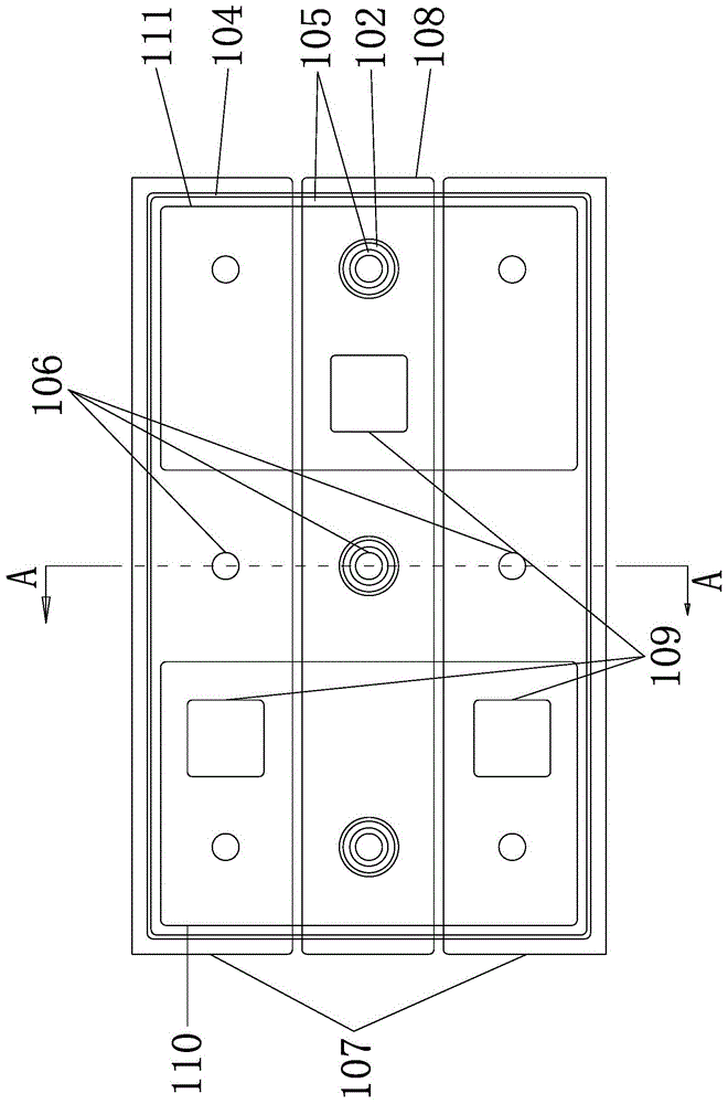
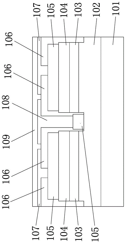
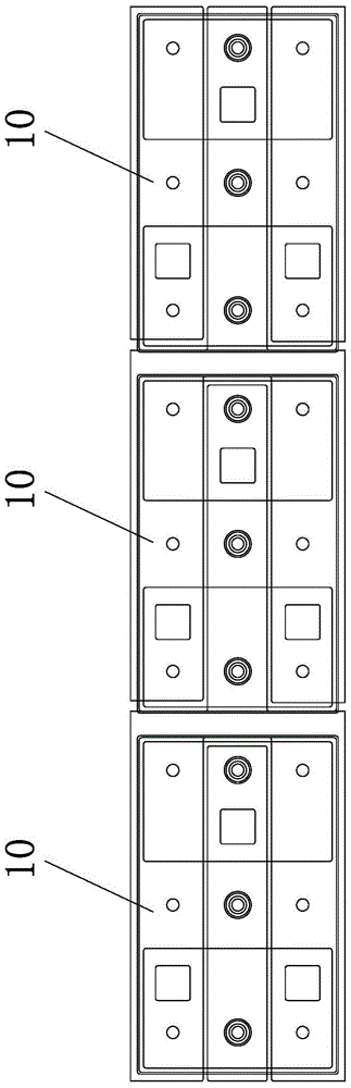
[0029] Such as Figure 1-2 Shown is a flip-chip light-emitting diode 10 with an ODR structure disclosed in the present invention, which mainly includes a substrate 101, an N-type layer 102, an active layer 103, a P-type layer 104, a current spreading layer 105, a DBR layer 106 and Ag reflective layer.

[0030] The N-type layer 102, the active layer 103 and the P-type layer 104 are sequentially arranged on the substrate 101, and the P-type layer 104 and the active layer 103 are etched to form steps to expose part of the N-type layer 102, the P-type layer 104 and the exposed A current spreading layer 105 is formed on the N-type layer 102 .

[0031] A DBR layer 106 is formed on the current spreading layer 105 , the DBR layer 106 is etched to expose a part of the current spreading layer 105 , and an Ag reflective...


PUM


Abstract

The invention discloses a flip light emitting diode (LED) with an ODR structure and a preparation method, and a flip high-voltage LED. According to the flip LED, an N type layer, an active layer and a P type layer are arranged on a substrate in sequence; a stage is formed through etching to expose a part of the N type layer; a current expansion layer is formed on the P type layer and the exposed N type layer; a DBR layer is formed on the current expansion layer; the DBR layer is etched to expose a part of the current expansion layer; an Ag reflection layer is formed on the DBR layer and the part of the exposed current expansion layer; and the Ag reflection layer is stripped to form a P contact metal layer and an N contact metal layer which are in ohmic contact with the current expansion layer on the P type layer and N type layer respectively. By adoption of the flip LED, the luminance of a chip is improved; extra metal evaporation is not required to form ohmic contact with an N-GaN layer, so that the technological steps and material are reduced, and the cost is low; and in addition, for the flip high-voltage LED, the Ag reflection layer can be used as high-reflection metal for forming the ODR structure, and also can be used as interconnecting metal between primitive cells, so that the technological steps are reduced, and the luminance of the chip is improved.

Description

technical field [0001] The invention relates to the technical field of light-emitting diodes, in particular to a flip-chip light-emitting diode with an ODR structure, a preparation method, and a flip-chip high-voltage LED. Background technique [0002] The structure of a flip-chip LED usually includes a substrate, an N-type layer, an active region, and a P-type layer arranged in sequence. Steps are formed by etching the LED chip, exposing the N-type layer, and forming on the surface of the unetched P-type layer. P electrode metal, N electrode metal is formed on the N-type stepped surface, and a mirror structure is arranged on the surface of the P-type layer. The mirror structure is covered with an insulating layer, and the insulating layer is a metal solder in contact with the electrode metal. plate. [0003] The current mainstream reflector structure is Ag structure, or DBR structure. For flip-chip LEDs with Ag structure, since Ag is an unstable metal, it is easy to oxidi...

Claims


Application Information

Patent Timeline
Patent Type & Authority Applications(China)
IPC IPC(8): H01L33/48H01L33/02H01L33/00
CPCH01L33/48H01L33/005H01L33/02
Inventor 周弘毅张永陈凯轩李俊贤刘英策陈亮魏振东李小平吴奇隆蔡立鹤邬新根黄新茂
Owner XIAMEN CHANGELIGHT CO LTD
Why Eureka
Try Eureka