High-fidelity and high-frequency circuit board

A high-frequency circuit board, circuit board technology, applied in the directions of printed circuits, printed circuits, printed circuit components, etc., can solve the problems of reducing the shielding effect at the opening, limiting the wiring of printed circuit boards, and limiting the shape of portable devices, etc. Excellent high and low temperature resistance, excellent electromagnetic shielding performance, good hydrophobic effect

Active Publication Date: 2016-11-30
惠州润众科技股份有限公司
View PDF6 Cites 0 Cited by
  • Summary
  • Abstract
  • Description
  • Claims
  • Application Information

AI Technical Summary

Problems solved by technology

For this reason, the shielding effect may be reduced at the opening, and the desire to route printed circuit board signal lines at this opening will be limited
Therefore, there is a problem that the connection form of the shielding material layer and the grounding part limits the wiring of the printed circuit board
In addition, the method of embedding the grounding part in the shielding material layer needs to expose the grounding part from the side of the shielding material layer, and there is a problem that the shape of the portable device suitable for the shielding material layer is limited.
[0004] In order to improve signal integrity and minimize production costs, the design and application of high-frequency and high-speed material mixed pressure and composite material mixed pressure embedded holes are in the ascendant; in order to install special function modules or simplify the design of electronic products, local embedding of high-density sub-boards, various High precision requires step board designs to emerge in endlessly; in the traditional PCB design process, if high-frequency signals need to be used, the design usually uses high-frequency materials to make the entire layer, which is expensive

Method used


Image

  • High-fidelity and high-frequency circuit board
  • High-fidelity and high-frequency circuit board
  • High-fidelity and high-frequency circuit board

Examples


Embodiment 1

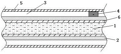
[0025] A high-fidelity high-frequency circuit board, the circuit board includes a circuit layer 1, and an insulating layer 2 arranged on the front and back of the circuit layer 1, and a layer of metal layer 3 is also arranged on the insulating layer 2, and the metal layer 3 on the top Layer 3 is partially laminated with a high-frequency sub-board 4 .

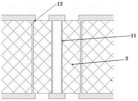
[0026] The circuit board also includes four first metal holes 11 arranged on the circuit board, and second metal holes 12 are respectively sleeved on the outer circumference of the first metal holes 11, and the second metal holes 12 and the first metal holes The holes 11 are concentric; the second metal hole 12 is grounded, and an insulating layer 2 is provided between the second metal hole 12 and the first metal hole 11 .

[0027] The surface of the metal layer 3 at the top or bottom is provided with a metal platinum coating 5, and the thickness of the metal platinum coating 5 is 4.5um.

[0028] The metal layer 3 is a metal fo...

Embodiment 2

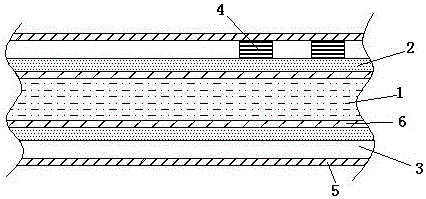
[0034] A high-fidelity high-frequency circuit board, the circuit board includes a circuit layer 1, and an insulating layer 2 arranged on the front and back of the circuit layer 1, and a layer of metal layer 3 is also arranged on the insulating layer 2, and the metal layer 3 on the top Layer 3 is partially laminated with two high-frequency sub-boards 4 .

[0035] The circuit board also includes four first metal holes 11 arranged on the circuit board, and second metal holes 12 are respectively sleeved on the outer circumference of the first metal holes 11, and the second metal holes 12 and the first metal holes The holes 11 are concentric; the second metal hole 12 is grounded, and an insulating layer 2 is provided between the second metal hole 12 and the first metal hole 11 .

[0036] The surface of the metal layer 3 at the top or bottom is provided with a metal platinum coating 5, and the thickness of the metal platinum coating 5 is 4um.

[0037] The metal layer 3 is a metal f...

Embodiment 3

[0043] A high-fidelity high-frequency circuit board, the circuit board includes a circuit layer 1, and an insulating layer 2 arranged on the front and back of the circuit layer 1, and a layer of metal layer 3 is also arranged on the insulating layer 2, and the metal layer 3 on the top Layer 3 is partially laminated with a high-frequency sub-board 4 .

[0044] The circuit board also includes four first metal holes 11 arranged on the circuit board, and second metal holes 12 are respectively sleeved on the outer circumference of the first metal holes 11, and the second metal holes 12 and the first metal holes The holes 11 are concentric; the second metal hole 12 is grounded, and an insulating layer 2 is provided between the second metal hole 12 and the first metal hole 11 .

[0045] The surface of the metal layer 3 at the top or bottom is provided with a metal platinum coating 5, and the thickness of the metal platinum coating 5 is 3um.

[0046] The metal layer 3 is a metal foil...


PUM


Abstract

The invention provides a high-fidelity and high-frequency circuit board. The circuit board comprises a circuit layer, and insulation layers arranged on the front and back of the circuit layer. At least one metal layer is arranged on each insulation layer. At least one high-frequency sub-board is in press fit with part of the metal layer located at the top.

Description

technical field [0001] The invention relates to the technical field of circuit boards, in particular to a high-fidelity high-frequency circuit board. Background technique [0002] In the 21st century, human beings have entered a highly informationized society, and PCB is an indispensable and important pillar in the information industry. Electronic equipment requires high performance, high speed, and miniaturization, and as a multidisciplinary industry, PCB is the most critical technology for high-end electronic equipment. Rigid, flexible, rigid-flexible multilayer boards in PCB products, as well as module substrates for IC packaging substrates, have made great contributions to high-end electronic equipment. The PCB industry occupies an important position in electronic interconnection technology. [0003] In recent years, along with the miniaturization of portable devices, personal computers, earphone jacks, and camera modules, there has been an increasing demand for miniat...

Claims


Application Information

Patent Timeline
Patent Type & Authority Applications(China)
IPC IPC(8): H05K1/02
CPCH05K1/0243H05K2201/0723
Inventor 杨美如乔鹏程胡立海赵宏静陈志宇
Owner 惠州润众科技股份有限公司
Why Eureka
Try Eureka