Stereoscopic structure organic semiconductor material and monomer preparation method

A technology of organic semiconductor and three-dimensional structure, which is applied in the fields of electricity and optics to achieve the effect of simple and convenient preparation process, simple preparation and reduced product cost

Inactive Publication Date: 2016-12-07
PEKING UNIV SHENZHEN GRADUATE SCHOOL
View PDF2 Cites 8 Cited by
  • Summary
  • Abstract
  • Description
  • Claims
  • Application Information

AI Technical Summary

Problems solved by technology

However, there are still many problems in the practical a

Method used


Image

  • Stereoscopic structure organic semiconductor material and monomer preparation method
  • Stereoscopic structure organic semiconductor material and monomer preparation method
  • Stereoscopic structure organic semiconductor material and monomer preparation method

Examples


Embodiment 1

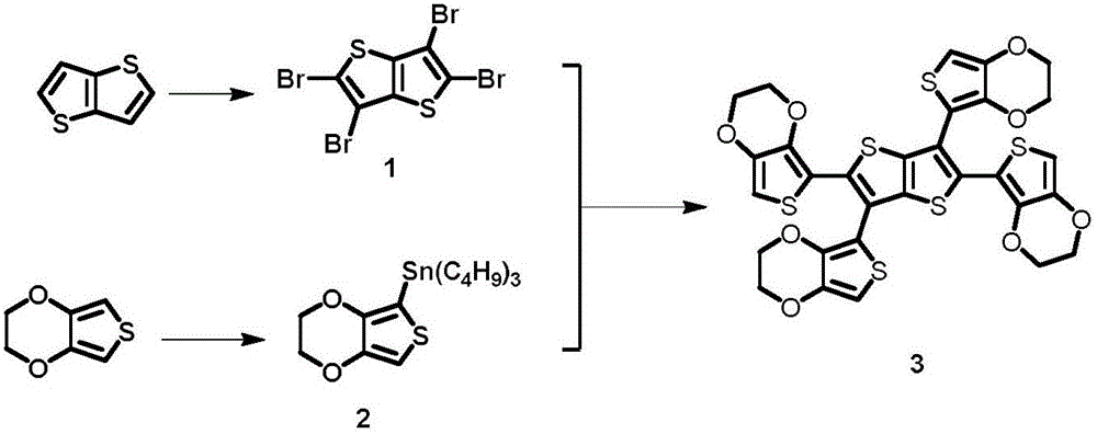
[0086] S1. Dissolve thiophene (5g, 35.7mmol) in a mixed solvent of glacial acetic acid (36ml) and chloroform (10ml), and add Br dropwise at room temperature 2 (28.5g, 180.56mmol), continue to stir for half an hour, and then heat and reflux overnight at 78°C; after cooling to room temperature, wash with water to precipitate a white solid compound, wash with water and methanol three times, and dry under vacuum at room temperature , to obtain white solid compound 1, [M+]=455.0. (yield: 95%);

[0087] S2, under the low temperature condition of -78 ℃, add n-BuLi (31.25ml) in the THF (150ml) solvent of EDOT (7.1g, 50mmol), stir at room temperature for 1.5 hours; Add ClSn (C 4 h 9 ) 3(50mmol, 13.56ml), reacted overnight at room temperature; quenched by adding saturated ammonium chloride solution, extracted with dichloromethane, and combined the organic phase; the organic phase was washed 3 times with water, dried over anhydrous magnesium sulfate, and spin-dried Distillation; Obtai...

Embodiment 2

[0090] The electrochemical polymerization process of monomer compound t-EDOT-TT is as follows:

[0091] In the electrodeposition process, the monomer compound t-EDOT-TT is first added to anhydrous dichloromethane solution to prepare a 0.56mM saturated solution, and then the electrolyte TBAPF is added to the solution 6 , so that the solution concentration is 0.1M. Using platinum wire as the counter electrode, ITO transparent glass as the working electrode, and silver wire as the reference electrode, the three-electrode system adopts cyclic voltammetry electropolymerization, and the voltage will be 100mV / s in the range of (-1.3V to +1.3V). The conductive polymer thin film deposited under the scan speed of 1 is marked as P(t-EDOT-TT)-1, and the conductive polymer thin film deposited under the same scan speed (-0.2V to 1.0V) is marked as P(t -EDOT-TT)-2;

Embodiment 3

[0093] The cyclic voltammetry scan of the monomer compound t-EDOT-TT is as follows:

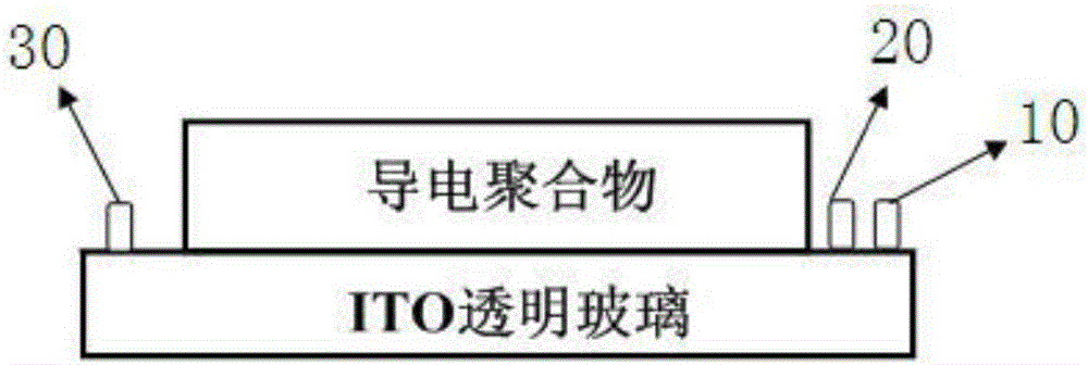
[0094] The platinum wire is used as the counter electrode, the ITO transparent glass is used as the working electrode, and the silver wire is used as the reference electrode. The film structure is as follows: image 3 Shown, wherein, 10 is a reference electrode, 20 is a counter electrode, and 30 is a working electrode; Cyclic voltammetry scanning obtains the cyclic voltammetry curves of two kinds of film polymers (i.e. conductive polymer films), as Figure 4a (corresponding to P(t-EDOT-TT)-1) and 4b (corresponding to P(t-EDOT-TT)-2); when the scanning speed is 100mV / s, P(t-EDOT-TT)-1 The starting point of oxidation is 0.26V, and the starting point of reduction is 0.094V. The oxidation onset of polymer P(t-EDOT-TT)-2 under the same conditions is 0.087V, and the reduction onset is -0.1V.


PUM


Abstract

The invention discloses a stereoscopic structure organic semiconductor material and a monomer preparation method. The structural formula of monomer of the stereoscopic structure organic semiconductor material is shown in the instruction. The preparation method is simple, a butterfly monomeric compound is obtained and has four different polymerization sites, so that the compound polymerized at different sites can be obtained under different polymerization conditions, and different types of stereoscopic polymer organic semiconductor materials are obtained. Thiophene or EDOT (ethylenedioxy thiophene) derivatives are added to a mother nucleus, HOMO (highest occupied molecular orbital) and LUMO (lowest unoccupied molecular orbital) energy levels of the material are further adjusted, the excellent organic semiconductor material is obtained, the preparation process is simple and convenient, product cost is greatly reduced, and a foundation is provided for application.

Description

technical field [0001] The invention relates to the fields of optics and electricity, in particular to a three-dimensional structure organic semiconductor material and a monomer preparation method. Background technique [0002] Organic semiconductor material is a kind of material with semiconducting properties. It has a wide range of applications in organic light-emitting diodes (OLEDs), perovskites, organic electrochromic (OEC), organic field-effect transistors (OTFT), and organic solar cells (OPV). application. [0003] For traditional inorganic semiconductor materials, such as silicon, germanium, gallium nitride, gallium arsenide, etc., technology has quickly entered the information age, showing its talents in the high-speed information age. Although inorganic semiconductor materials have shown many advantages in the development of science and technology, there are still limitations in inorganic semiconductor materials, such as relatively single types of materials, compl...

Claims


Application Information

Patent Timeline
IPC IPC(8): C07D495/14C07D333/08C07D409/14C07D495/04C07D519/00C25B3/00
CPCC07D495/14C07D333/08C07D409/14C07D495/04C07D519/00C25B3/00
Inventor 孟鸿史晶晶
Owner PEKING UNIV SHENZHEN GRADUATE SCHOOL
Why Eureka
Try Eureka