Method for depositing nano-silver in microfluidic channels

A nano-silver, microfluidic technology, applied in chemical instruments and methods, laboratory containers, instruments, etc., can solve problems such as complex process conditions and the use of expensive instruments, and achieve good repeatability, low price, and repeatability. high effect

Active Publication Date: 2016-12-07
DALIAN UNIVERSITY
View PDF3 Cites 18 Cited by
  • Summary
  • Abstract
  • Description
  • Claims
  • Application Information

AI Technical Summary

Problems solved by technology

[0003] The purpose of the present invention is to overcome the deficiencies in the prior art, provide a kind of with (PDDA/PSS) n Multilayer self-assembled film of ITO glass as the substrate, with NaNO 3 and AgNO

Method used


Image

  • Method for depositing nano-silver in microfluidic channels
  • Method for depositing nano-silver in microfluidic channels
  • Method for depositing nano-silver in microfluidic channels

Examples


Embodiment 1

[0021] (1) Pour PDMS liquid A (monomer) and liquid B (initiator) into a beaker at a mass ratio of 10:1, stir with a glass rod for 5 minutes, and then pour it into the above-mentioned petri dish with a silicon wafer.

[0022] (2) Put the petri dish in a concentrated desiccator, pump air with a diaphragm vacuum pump for 1.5 hours to remove air bubbles in PDMS, and then place it in a vacuum oven at 80° C. for 1 hour to solidify.

[0023] (3) After it cools naturally, gently peel off the PDMS from the silicon wafer template, cut it into small pieces with a cutting machine, and then punch holes in the corresponding parts with a manual chip puncher for experimental use.

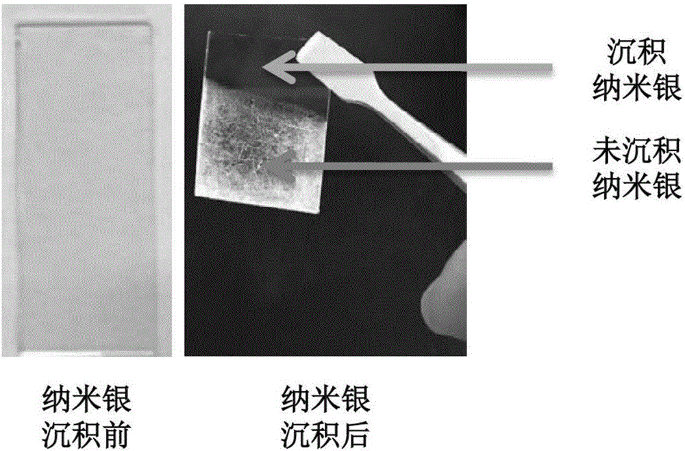
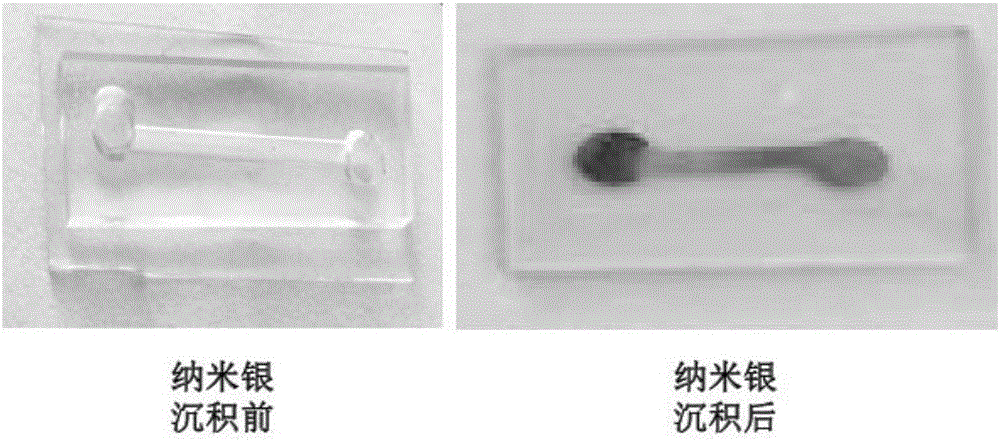
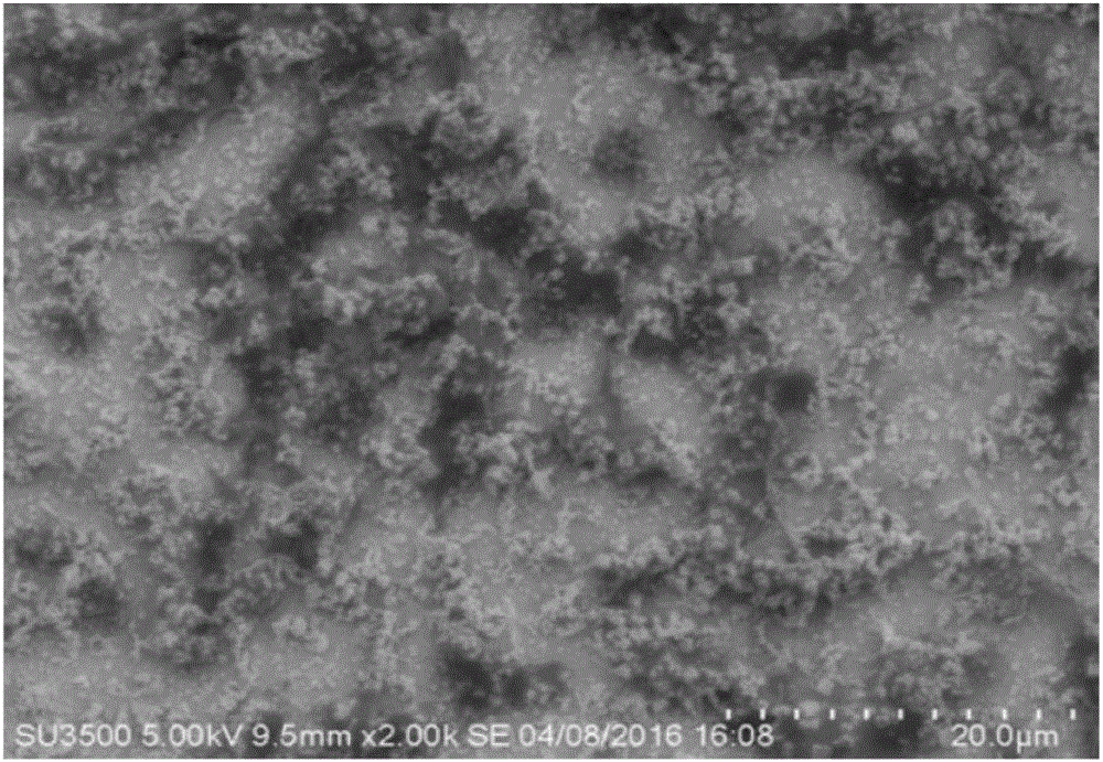
[0024] (4) Ultrasonic clean the ITO glass with absolute ethanol, and then place it in a UV ozone cleaner for 30 minutes, then place the cleaned ITO with the conductive surface facing up, soak it in 1 mg / mL PDDA solution for 5 minutes, and take it out , washed with distilled water several times in a small amount, an...

Embodiment 2

[0032] (1) Pour PDMS liquid A (monomer) and liquid B (initiator) into a beaker at a mass ratio of 10:1, stir with a glass rod for 5 minutes, and then pour it into the above-mentioned petri dish with a silicon wafer. The culture dish was placed in a concentrated desiccator, evacuated with a diaphragm vacuum pump for 1.5 hours to remove air bubbles in PDMS, and then placed in a vacuum oven at 80°C for 1 hour to solidify. After it cooled naturally, the PDMS was gently peeled off from the silicon wafer template, cut into small pieces with a cutting machine, and then punched holes in the corresponding parts with a manual chip puncher for experimental use.

[0033] (2) Ultrasonic clean the ITO glass with absolute ethanol, and then place it in a UV ozone cleaner for 30 minutes, then place the cleaned ITO with the conductive surface facing up, soak it in 1 mg / mL PDDA solution for 5 minutes, and take it out , washed with distilled water several times in a small amount, and then blown d...

Embodiment 3

[0037] (1) Pour PDMS liquid A (monomer) and liquid B (initiator) into a beaker at a mass ratio of 10:1, stir with a glass rod for 5 minutes, and then pour it into the above-mentioned petri dish with a silicon wafer. The culture dish was placed in a concentrated desiccator, evacuated with a diaphragm vacuum pump for 1.5 hours to remove air bubbles in PDMS, and then placed in a vacuum oven at 80°C for 1 hour to solidify. After it cooled naturally, the PDMS was gently peeled off from the silicon wafer template, cut into small pieces with a cutting machine, and then punched holes in the corresponding parts with a manual chip puncher for experimental use.

[0038] (2) Ultrasonic clean the ITO glass with absolute ethanol, and then place it in a UV ozone cleaner for 30 minutes, then place the cleaned ITO with the conductive surface facing up, soak it in 1 mg / mL PDDA solution for 5 minutes, and take it out , washed with distilled water several times in a small amount, and then blown d...


PUM


Abstract

The invention relates to a method for depositing nano-silver in microfluidic channels. The method comprises the steps that ITO glass is pretreated, and ITO glass with (PDDA/PSS) n multilayer self-assembled films is prepared; the ITO glass serves as a substrate and is connected with a chip made of PDMS in an encapsulating mode to form a microfluidic chip, then a NaNO3 and AgNO3 mixed solution is injected into microfluidic channels, nano-silver is deposited in the microfluidic channels with chronoamperometry, and nano-silver surface morphology detection shows that nano-silver particles distributed evenly can be seen in the microfluidic channels. The method has the advantages of being quick, simple, high in repeatability, low in cost and the like, and has wide application prospects in the fields such as medical bio-engineering and medical biosensors.

Description

technical field [0001] The invention relates to a microfluidic channel surface treatment technology, in particular to a process method for depositing nano-silver in a microfluidic channel. Background technique [0002] With the rapid development of life sciences, and life science research from macro to micro, analytical instruments and analytical science have also undergone profound changes. In order to meet the needs of the development of life sciences from macro to micro, the development trend of analytical instruments is becoming more and more integrated, miniaturized and portable. Microfluidics is a technology platform that can effectively concentrate the functions of ordinary instruments on a chip of a few square centimeters in size. Microfluidic chips have been widely used in biochemistry, medical examination, drug synthesis, screening, environmental monitoring and other fields, with a wide range of applications and applications. Nano-silver refers to silver particle...

Claims


Application Information

Patent Timeline
IPC IPC(8): G01N27/26G01N27/30B01L3/00C25D3/46C25D7/04
CPCB01L3/5027B01L2200/10B01L2300/0887B01L2300/12C25D3/46C25D7/04G01N27/26G01N27/30G01N27/307
Inventor 孙晶郎明非
Owner DALIAN UNIVERSITY
Why Eureka
Try Eureka