Check patentability & draft patents in minutes with Patsnap Eureka AI!

Array waveguide grating with channel monitoring function

An arrayed waveguide grating and channel monitoring technology, applied in the field of communication, can solve the problems of large and complex chips, unfavorable productization, and complex implementation, and achieve the effect of simple process and compact structure

Inactive Publication Date: 2016-12-07
GUANGXUN SCI & TECH WUHAN
View PDF17 Cites 2 Cited by
  • Summary
  • Abstract
  • Description
  • Claims
  • Application Information

AI Technical Summary

Problems solved by technology

The scheme of thinning the waveguide cladding requires an additional process of photolithography and overlay; the scheme of using the second AWG makes the chip too large and complicated; the scheme of using different diffraction orders and output waveguide coupling and splitting needs to AWG for special design
The realization of these technical solutions is too complicated, which is not conducive to productization

Method used


Image

  • Array waveguide grating with channel monitoring function
  • Array waveguide grating with channel monitoring function
  • Array waveguide grating with channel monitoring function

Examples


Embodiment Construction

[0036] The arrayed waveguide grating with channel monitoring function of the present invention will be described in detail below in conjunction with the embodiments.

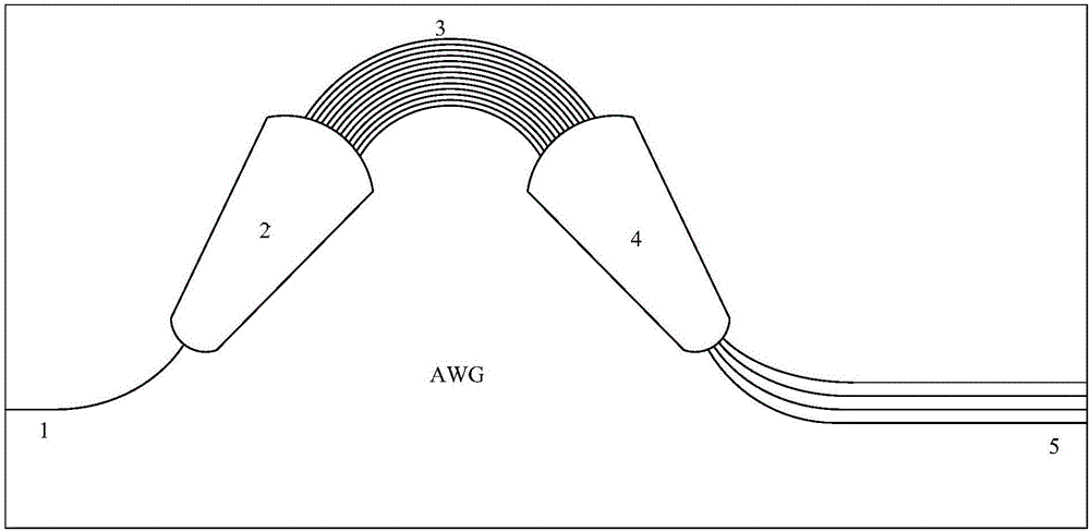
[0037] The present invention proposes an arrayed waveguide grating with channel monitoring function, including AWG and PLC type optical couplers, AWG and PLC type optical couplers are integrated on the same waveguide substrate, and the AWG input waveguide or output waveguide needs to be monitored The channel is equipped with a PLC type optical coupler.

[0038] The technical problem to be solved by the present invention is to simplify the AWG chip design and the complexity of the manufacturing process, and realize the AWG with channel monitoring function through the scheme of monolithically integrating the optical coupler on the chip, so as to meet the practical requirements of large-scale production. need. Taking the multiplexer as an example, light with wavelengths of λ1, λ2, λ3, and λ4 enters the 4 input wav...


PUM


Abstract

The invention provides an array waveguide grating with a channel monitoring function. The array waveguide grating comprises an AWG and a PLC type split light coupler which are integrated on a same waveguide substrate, and the PLC type split light coupler is arranged on a channel, needing to be monitored, of an input waveguide or output waveguide of the AWG. According to the device, an additional chip manufacturing process is not added, special design on the AWG is not needed, the process is simple, and the large-scale production requirements are met; integration of the split light coupler with a monitoring function and the AWG single chip is achieved, and the structure is compact.

Description

technical field [0001] The invention relates to an arrayed waveguide grating with channel monitoring function, which belongs to the communication field. Background technique [0002] With the completion of 40 / 100 Gigabit Ethernet (GbE) optical interface standard (IEEE802.3ba-2010) and pluggable optical transceiver module standard (CFP-MAS Rev 1.4), and the first generation of 40GbE / 100GbE CFP products Gradually entering the market, manufacturers are gradually shifting their attention to the R&D and design of 40 / 100GbE pluggable transceivers. For system manufacturers and customers, module power consumption and size are the key indicators to increase system port density and reduce the cost of the entire optical port, so it has become the primary goal of R&D and design, and the monolithic integrated waveguide solution is the mainstream implementation solution. [0003] IEEE 802.3ba-2010 defines the most widely used 40GBase-LR4 optical interface working at 1310nm, 4-wavelength ...

Claims


Application Information

Patent Timeline
IPC IPC(8): G02B6/12
CPCG02B6/12019G02B6/12033
Inventor 马卫东周天红张冀李迪
Owner GUANGXUN SCI & TECH WUHAN
Features
  • R&D
  • Intellectual Property
  • Life Sciences
  • Materials
  • Tech Scout
  • Unparalleled Data Quality
  • Higher Quality Content
  • 60% Fewer Hallucinations
Learn More