Method for SOC (system on chip) asynchronous clock domain signal interface

A signal interface and asynchronous clock technology, applied in the field of VLSI and integrated circuits

Active Publication Date: 2016-12-07
CENT SOUTH UNIV
View PDF5 Cites 1 Cited by
  • Summary
  • Abstract
  • Description
  • Claims
  • Application Information

AI Technical Summary

Problems solved by technology

[0005] The purpose of the present invention is to solve the problem of SOC asynchronous clock domain signal interface, and propose a simple and reliable method for the above four aspects, which can solve the problem of metastable state, and has no input pulse width limitation

Method used


Image

  • Method for SOC (system on chip) asynchronous clock domain signal interface
  • Method for SOC (system on chip) asynchronous clock domain signal interface
  • Method for SOC (system on chip) asynchronous clock domain signal interface

Examples


Embodiment Construction

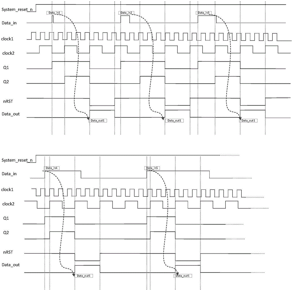
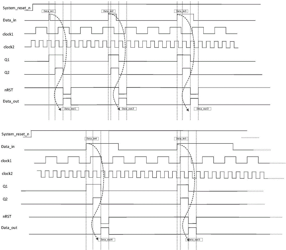
[0020] The present invention will be further described in detail below in conjunction with the accompanying drawings and specific embodiments.

[0021] 1. Explanation of circuit connection, device function, and signal naming:

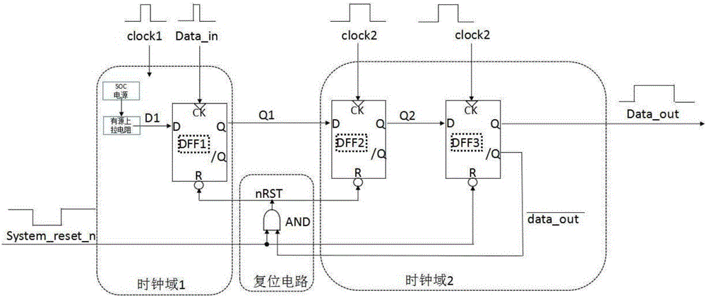
[0022] Such as figure 1 As shown, the circuit uses 4 devices, three latches and one gate unit.

[0023] They are respectively: the first latch DFF1, the second latch DFF2, the third latch DFF3, and the gate unit AND. The type of latch is: synchronous flip-flop with asynchronous reset terminal. The asynchronous reset terminal is defined as R, the synchronous clock terminal is defined as CK, the data input terminal is named D, the data output terminal is named Q, and the inverted data output terminal is named / Q. The input terminals include: D, R, CK; the output terminals include: Q, / Q. The function description is as follows: asynchronous reset terminal R, when input low level "0" (other input terminals can be any value), Q terminal output low, / Q ou...


PUM


Abstract

The invention relates to a method for an SOC (system on chip) asynchronous clock domain signal interface and relates to a design method of the very large scale integration (VLSI) field. The method comprises a clock domain (1), a clock domain (2) and a reset circuit, wherein an input data pulse signal is transmitted to the clock domain (2) from the clock domain (1); the clock domain (1) comprises a first data latch; the clock domain (2) comprises a second data latch and a third data latch; and the reset circuit is mainly composed of one and gate. All the devices in the clock domain (1) realize latching of the input data pulse signal; the devices in the clock domain (2) realize the effects of synchronizing the signal and producing a feedback signal; and the reset circuit eliminates information latched by the first data latch and the second data latch in time according to the feedback signal of the clock domain (2). The method provided by the invention has the advantages that structure is simple, in SOC clock domain crossing design, transmission of two asynchronous clock domain signals can be realized, and metastable state effect is eliminated.

Description

technical field [0001] The invention relates to the field of integrated circuits, in particular to a design method in the field of very large scale integrated circuits (VLSI). Background technique [0002] With the passage of time, the integrated circuit industry has developed to 2016, and advanced foundries like Intel have proposed plans to enter the 10nm process. The promotion of high integration has also made the scale of the chip larger and larger, the functions more and more complex, and the design difficulty is getting higher and higher. [0003] The complexity of the internal clock of the SOC leads to more and more interfaces across clock domains. For the processing of these asynchronous signals, foreign pioneers put forward many constructive suggestions, which pointed out the way for our domestic practitioners. Generally speaking, it can be divided into two categories: using latches and combined devices to process; the other is to use FIFO as an interface cache. ...

Claims


Application Information

Patent Timeline
Patent Type & Authority Applications(China)
IPC IPC(8): G06F13/38
CPCG06F13/385Y02D10/00
Inventor 梁步阁张岩松张锋容睿智赵旸
Owner CENT SOUTH UNIV
Why Eureka
Try Eureka