Method of manufacturing wafer

A production method and wafer technology, applied in chemical instruments and methods, crystal growth, single crystal growth, etc., can solve problems such as operation process exposure, metal element diffusion, wafer electrical changes, etc., to avoid wafer cracking, Reduce the effect of metal element diffusion

Inactive Publication Date: 2016-12-07
KUNSHAN ZHONGCHEN SILICON CO LTD
View PDF8 Cites 4 Cited by
  • Summary
  • Abstract
  • Description
  • Claims
  • Application Information

AI Technical Summary

Problems solved by technology

In addition, halogen gas may expose the operation process to a toxic environment, and there are doubts about safety issues
High temperature may cause a large diffusion of metal elements, resulting in electrical changes in the wafer, which cannot meet the specifications

Method used


Image

  • Method of manufacturing wafer
  • Method of manufacturing wafer
  • Method of manufacturing wafer

Examples


Embodiment Construction

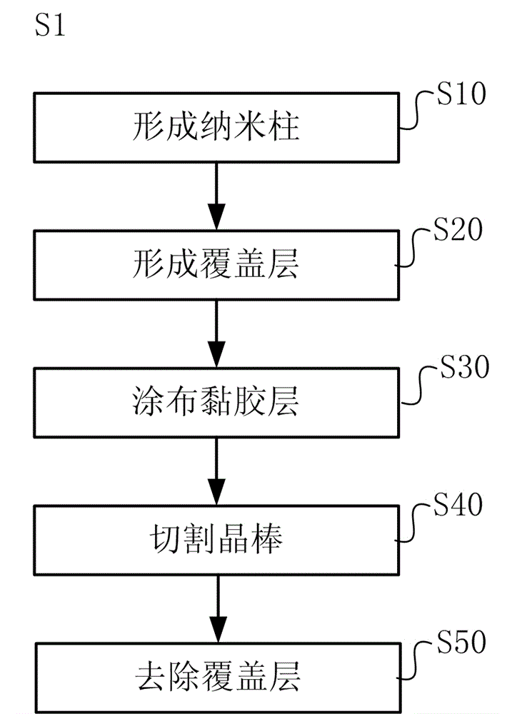
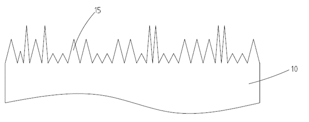
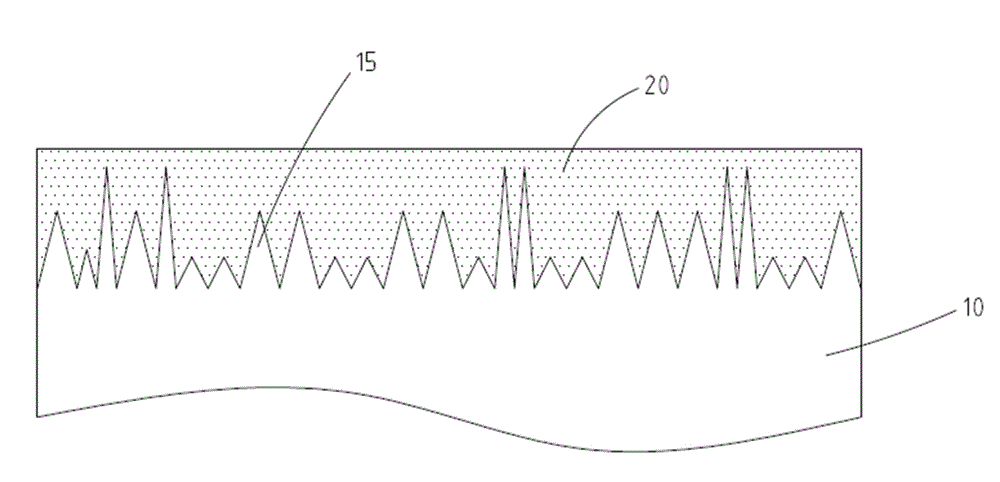
[0021] refer to Figure 1-Figure 6 , figure 1 It is a flow chart of the wafer manufacturing method of the present invention, Figure 2 to Figure 6 It is a step-by-step partial cross-sectional schematic diagram of the wafer manufacturing method of the present invention. Such as figure 1 As shown, the wafer manufacturing method S1 of the present invention includes step S10, step S20, step S30, step S40 and step S50. The steps will be coordinated with Figure 2 to Figure 6 The cross-section is shown to illustrate.

[0022] Step S10 is to form nanopillars. Such as figure 2 As shown, step S10 is to form a plurality of nanopillars 15 on the surface of the crystal rod 10 . The ingot 10 may be a silicon ingot, a sapphire ingot, or the like. The method of forming the nano-column 15 is chemical etching or chemical deposition, which are just examples and are not limited thereto. The width of the nanopillar 15 is 10-600 nm, preferably 40-400 nm. The length of the nanopillars is...


PUM

PropertyMeasurementUnit
lengthaaaaaaaaaa
lengthaaaaaaaaaa

Abstract

The invention provides a method of manufacturing a wafer. A method of manufacturing a wafer includes a step for forming nanorods on the surface of an ingot, a step for forming a coating layer covering the nanorods on the surface of the ingot, a step for forming an adhesive layer on the surface of the coating layer, a step for cutting the ingot as a plurality of wafers, and a step for removing the coating layer and adhesive layer on the wafer simultaneously, with a solvent causing chemical action on the coating layer, but not causing chemical action on the wafer. Since the nanorods are covered by forming a coating layer, and the coating layer can be removed by chemical reaction, problem of residual adhesive can be solved. Furthermore, since the method can be operated under low temperature environment, the problem of exposure to a toxic environment in the operation flow is solved, while reducing diffusion phenomenon of metal elements.

Description

technical field [0001] The invention relates to a wafer process, in particular to a method for cutting crystal rods into wafers. Background technique [0002] Wafers are formed by dicing boules. If there is stress concentration during ingot cutting, it is easy to cause damage and fragmentation of the wafer. For example, for solar polysilicon wafers, if there is a problem of stress concentration, it may cause wafer cracks. Although it can be recycled, it will greatly increase the production cost. [0003] With the development of nanotechnology, we can understand that the surface area increases, which can effectively distribute stress. For the cutting of ingots, nanotechnology is used to develop nano-column structures on the surface of ingots to disperse stress and improve cutting yield. However, when the ingot is cut, the surface of the ingot is usually coated with an adhesive to fix it on the cutting machine, which is accompanied by side effects. When the nanopillar str...

Claims


Application Information

Patent Timeline
Patent Type & Authority Applications(China)
IPC IPC(8): H01L21/02
CPCH01L31/00C30B29/06C30B33/06
Inventor 叶哲良庄志远范俊一徐文庆
Owner KUNSHAN ZHONGCHEN SILICON CO LTD
Why Eureka
Try Eureka