Thick-film SOI-LIGBT device and method for improving latch-up resistance thereof

A device and thick film technology, which is applied in semiconductor devices, semiconductor/solid-state device manufacturing, electrical components, etc., can solve the problem that devices cannot be turned off, so as to improve the ability to resist latch-up, reduce the voltage drop, and reduce the possibility of latch-up sexual effect

Active Publication Date: 2016-12-21
SOUTHEAST UNIV
View PDF3 Cites 4 Cited by
  • Summary
  • Abstract
  • Description
  • Claims
  • Application Information

AI Technical Summary

Problems solved by technology

The hole current is sent from the anode and flows through the N-type buffer zone, N-type drift region and P-type body region, and finally collected by the cathode P-type contact region; when the hole current is too large, it will flow through the lateral groove in the P-type body region When the voltage drop in the channel area reaches 0.7V, the parasitic NPN transistor is turned on. At this time, the parasitic NPN transistor and the PNP transistor at the collector provide base current to each other, so that the device cannot be turned off, and finally a latch-up phenomenon is formed.

Method used


Image

  • Thick-film SOI-LIGBT device and method for improving latch-up resistance thereof
  • Thick-film SOI-LIGBT device and method for improving latch-up resistance thereof
  • Thick-film SOI-LIGBT device and method for improving latch-up resistance thereof

Examples


Embodiment 1

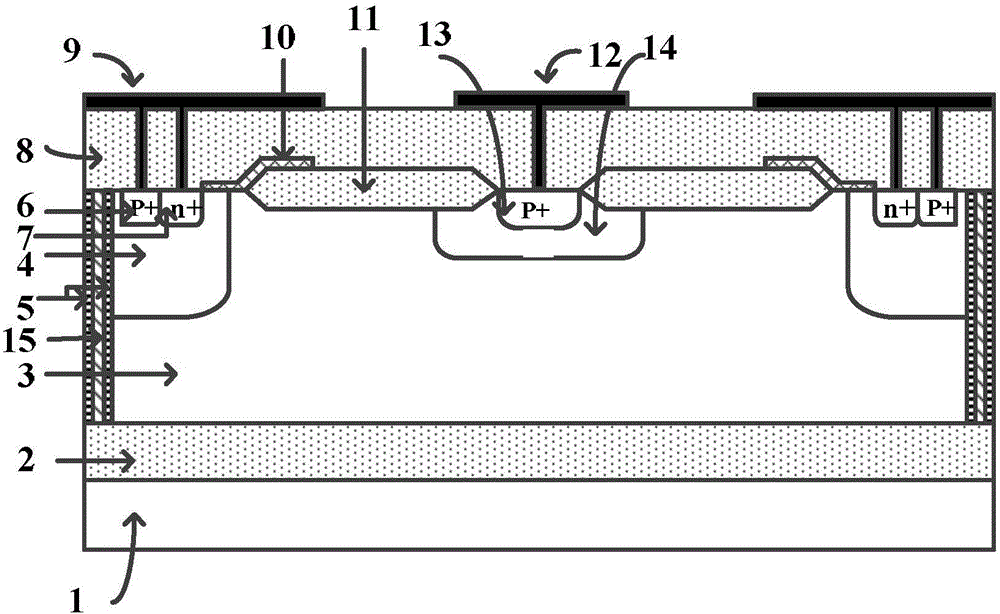
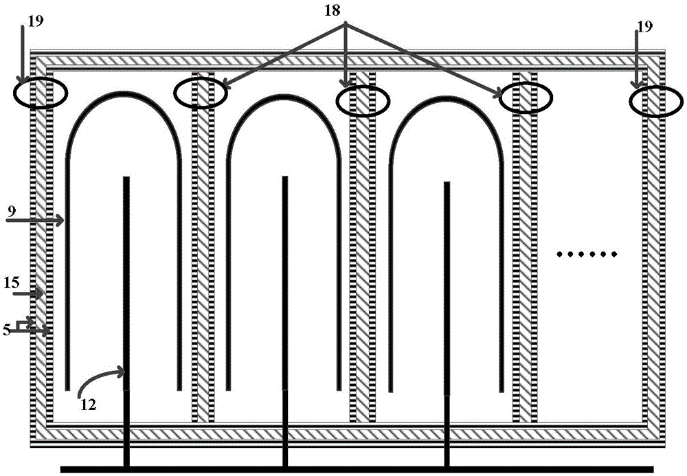
[0021] A thick-film SOI-LIGBT device, comprising a P-type substrate 1, a layer of buried oxide layer 2 is arranged on the P-type substrate 1, an N-type drift region 3 is arranged above the buried oxide layer 2, and the N-type drift region 3 P-type body region 4 and N-type buffer zone 14 are provided inside, and P-type cathode contact region 6 and n-type cathode contact region 7 are arranged on the surface of P-type body region 4, and P-type cathode contact region 6 and n-type cathode contact region 7 is connected to the cathode contact metal layer 9, a P-type anode contact region 13 is provided on the surface of the N-type buffer zone 14, the P-type anode contact region 13 is connected to the anode contact metal layer 12, and the surface of the N-type drift region 3 has field oxidation Layer 11 and conductive polysilicon gate 10, field oxide layer 11 is between n-type cathode contact region 7 and P-type contact region 13, conductive polysilicon gate 10 extends from the boundary...

Embodiment 2

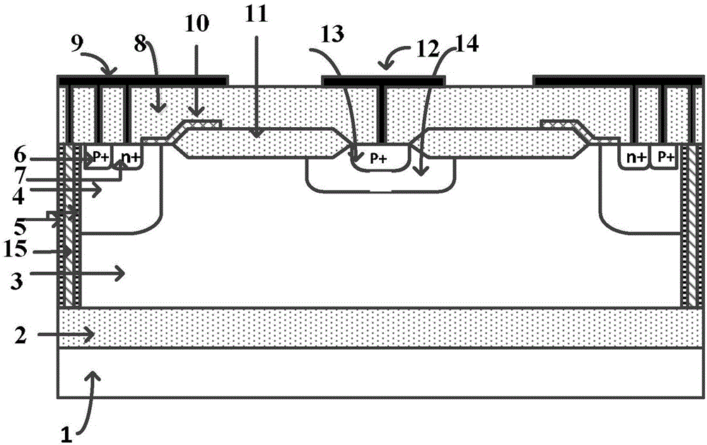
[0023]A method for improving the latch-up resistance of the thick-film SOI-LIGBT device, the SOI-LIGBT device includes a P-type substrate 1, a layer of buried oxide layer 2 is arranged on the P-type substrate 1, and the buried oxide There is an N-type drift region 3 above the layer 2, and a P-type body region 4 and an N-type buffer zone 14 are arranged inside the N-type drift region 3, and a P-type cathode contact region 6 and an n-type cathode are arranged on the surface of the P-type body region 4 The contact area 7, the P-type cathode contact area 6 and the n-type cathode contact area 7 are connected to the cathode contact metal layer 9, and the surface of the N-type buffer zone 14 is provided with a P-type anode contact area 13, and the P-type anode contact area 13 is connected to the anode The contact metal layer 12 is connected, the surface of the N-type drift region 3 has a field oxide layer 11 and a conductive polysilicon gate 10, the field oxide layer 11 is between the...


PUM

PropertyMeasurementUnit
Doping concentrationaaaaaaaaaa

Abstract

The invention provides a thick-film SOI-LIGBT device and a method for improving latch-up resistance thereof. The device comprises a P-type substrate. A buried oxide layer is arranged on the P-type substrate. An N-type drift region is arranged above the buried oxide layer. A P-type body region and an N-type buffer region are arranged inside the N-type drift region. A P-type cathode contact region and an n-type cathode contact region are provided on the surface of the P-type body region. The contact region is connected with the cathode contact metal layer. A P-type anode contact region is arranged on the surface of the N-type buffer region. The contact region is connected with the anode contact metal layer. A field oxide layer and a conductive polysilicon gate are arranged on the surface of the N-type drift region. Passivation layers are arranged on the surface of the cathode contact region, the anode contact region, the field oxide layer and the conductive polysilicon gate. The device is characterized in that an isolation trench is arranged on the outside of the cathode of the device; and conductive polysilicon in the isolation trench is shorted to the cathode contact region and the cathode metal layer. According to the method, the potential difference between the conductive polysilicon in the isolation trench and the N-type drift region is increased; hole current flowing through a lateral channel in the P-type body region is reduced; and the latch-up resistance is improved.

Description

technical field [0001] The invention relates to the reliability field of integrated circuits, and relates to a thick-film SOI-LIGBT device and a method for improving its anti-latch ability. Background technique [0002] High-power semiconductor devices and integrated circuits have accounted for about 75% of the total value of the international power semiconductor industry. my country's independent research and development of high-power device technology is also gradually internationalized. At the same time, reliability issues such as overheating, overvoltage, electrostatic protection (ElectronicStatic Discharge protection, ESD), and anti-latch-up of devices are also particularly prominent. Among them, the overcurrent problem caused by the latch-up effect makes the insulated gate bipolar transistor (Insulated Gate Bipolar Transistor, IGBT), silicon-on-insulator lateral insulated gate bipolar transistor (Silicon-On-Insulated-Lateral Insulated Gate Bipolar Transistor, SOI- LIG...

Claims


Application Information

Patent Timeline
IPC IPC(8): H01L29/739H01L29/06H01L21/331
CPCH01L29/0684H01L29/66325H01L29/7393
Inventor 孙伟锋李秀军叶然魏家行杨翰琪刘斯扬陆生礼时龙兴
Owner SOUTHEAST UNIV
Why Eureka
Try Eureka