Thin chip machining and pasting assembly method

An assembly method and thin chip technology, applied in the field of microelectronics, can solve the problems of complicated operation, many processes, and high price of cutting protective film, and achieve the effect of less process, easy debonding, and reduction of equipment precision requirements.

Inactive Publication Date: 2017-01-11
ZHEJIANG MICROTECH MATERIAL CO LTD
View PDF3 Cites 4 Cited by
  • Summary
  • Abstract
  • Description
  • Claims
  • Application Information

AI Technical Summary

Problems solved by technology

[0003] It is not difficult to see that in the process of processing and patch assembly of this thin chip in the prior art, there are not only many procedures and complex operations, but also the price of the cutting protective film used is relatively high.

Method used


Image

  • Thin chip machining and pasting assembly method
  • Thin chip machining and pasting assembly method
  • Thin chip machining and pasting assembly method

Examples


Embodiment Construction

[0034] The present invention will be further described below in conjunction with the accompanying drawings and specific embodiments.

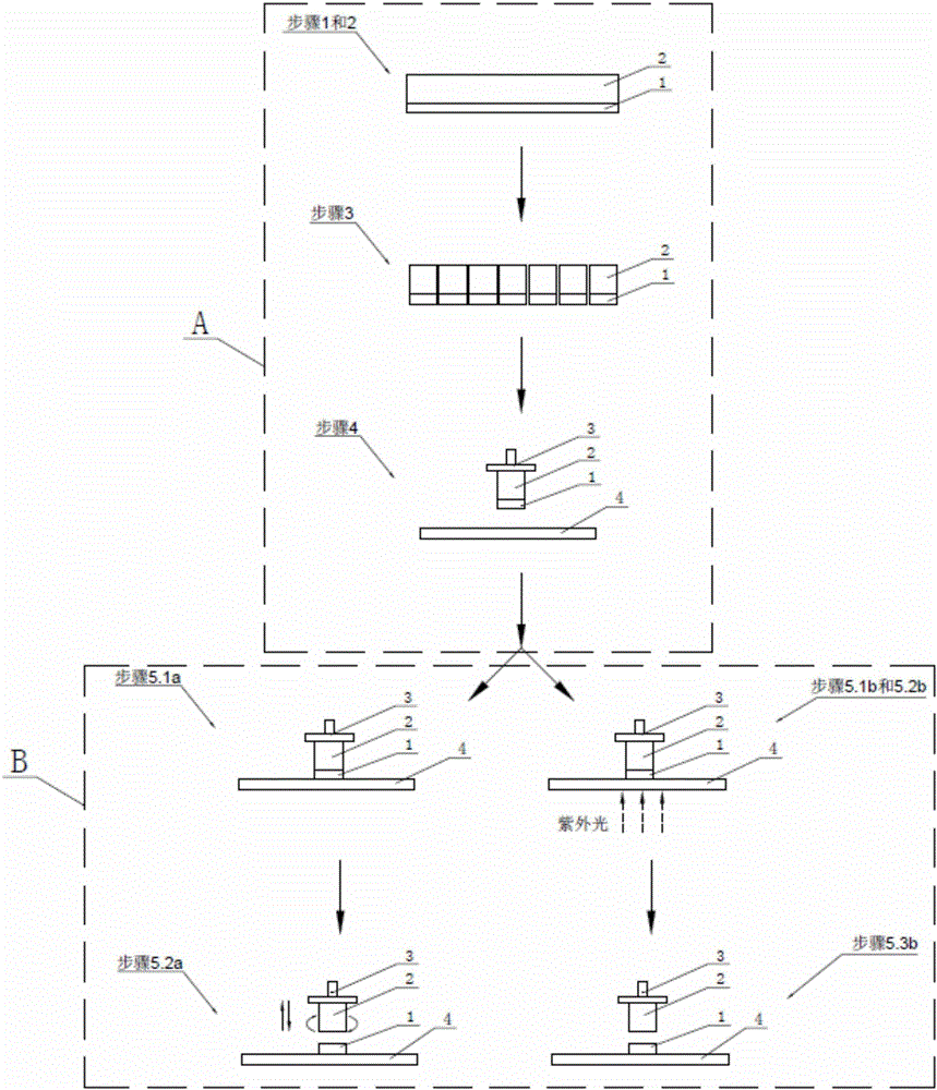
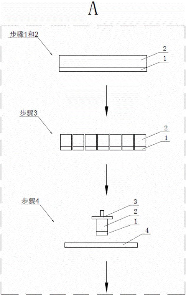
[0035] The invention provides a thin chip processing and patch assembly method, which includes:

[0036] Step 1, bonding the functional wafer 1 and the carrier wafer 2 through a bonding glue;

[0037] Step 2, thinning the functional wafer 1;

[0038] It is characterized in that: it also includes:

[0039] Step 3, cutting the functional wafer 1 and the carrier wafer 2 into several subunits; each subunit includes a small functional wafer 1 and a carrier wafer 2 .

[0040] Step 4, grabbing the carrier wafer 2 in the subunit by the clamping mechanism 3 and moving it to the corresponding substrate 4;

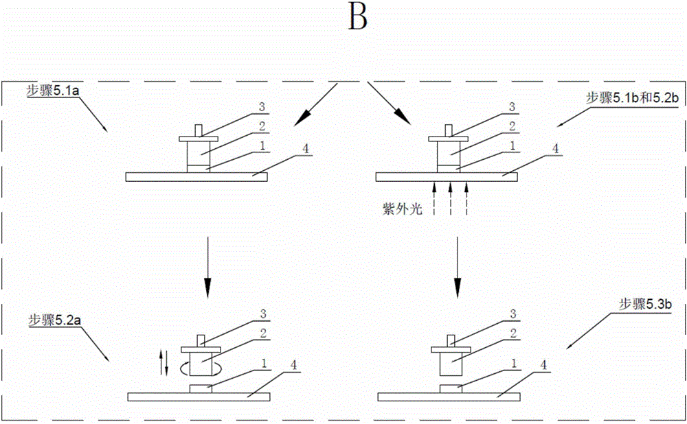
[0041] Step 5, the functional wafer 1 in the subunit is bonded to the substrate 4 , and the functional wafer 1 and the carrier wafer 2 are driven to debond during the process of pulling the clamping mechanism 3 away.

[0042] Said step 5 includes:...


PUM


Abstract

The invention discloses a thin chip machining and pasting assembly method, and the method comprises the following steps: 1, bonding a functional wafer and a carrier wafer through a bonding adhesive; 2, thinning the functional wafer; 3, cutting the functional wafer with the carrier wafer cut into several sub-units; 4, clamping the carrier wafer in the sub-unit through a clamping mechanism and enabling the carrier wafer move to a corresponding substrate; 5, bonding the functional wafer in the sub-units and the substrate, and carrying out the de-bonding of the functional wafer and the carrier wafer in an extraction process of the clamping mechanism. The method can reduce the processing steps without affecting the quality of the wafer, and there is no need of additional chip taking tools and thin chip fixtures, so the processing efficiency is high and the processing cost is low.

Description

technical field [0001] The invention relates to the technical field of microelectronics, in particular to a thin chip processing and chip assembly method. Background technique [0002] The so-called thin chip processing refers to cutting the entire wafer into the required size after thinning and other processing in the industry, and the thinned and cut granular wafer is Finally, the cut thin chips are installed on the corresponding substrate one by one, so as to complete the processing and placement of the thin chips. Since the entire wafer after thinning is extremely fragile, the wafer needs to be bonded to the carrier during the thinning process. Therefore, the processing method for the wafer in the existing industry simply includes the following steps, 1. ) The whole wafer is bonded on the carrier through bonding glue, 2) The whole wafer is thinned and processed by other processes, 3) The carrier and the thinned wafer are attached to the dicing film, 4) Debonding and re...

Claims


Application Information

Patent Timeline
Patent Type & Authority Applications(China)
IPC IPC(8): H01L21/78H01L21/683
CPCH01L21/78H01L21/6835H01L2221/68318H01L2221/68327H01L2221/68354H01L2221/68381
Inventor 唐昊
Owner ZHEJIANG MICROTECH MATERIAL CO LTD
Why Eureka
Try Eureka