An LC low-pass filter based on TSV array

A low-pass filter and through-silicon via technology, applied in the field of passive devices, to achieve the effect of eliminating electromagnetic radiation and coupling noise, large inductance value, and small chip area occupation

Active Publication Date: 2018-12-11
XIDIAN UNIV
View PDF4 Cites 0 Cited by
  • Summary
  • Abstract
  • Description
  • Claims
  • Application Information

AI Technical Summary

Problems solved by technology

At present, microwave components are developing in the direction of miniaturization and multi-functional integration. In many applications, they need to be system-integrated with common CMOS active circuits to realize various system modules with high functional integration. However, the existing Microwave components are not yet up to the mark

Method used


Image

  • An LC low-pass filter based on TSV array
  • An LC low-pass filter based on TSV array
  • An LC low-pass filter based on TSV array

Examples


Embodiment Construction

[0031] The following describes the present invention in detail with reference to the drawings and specific embodiments.

[0032] 1. The structure of LC low-pass filter based on silicon through hole array

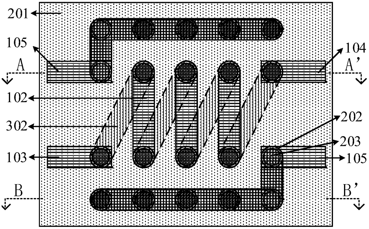
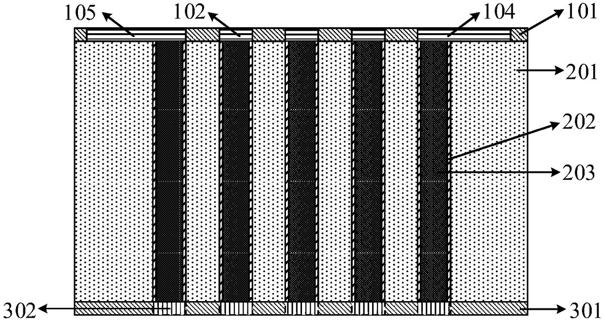
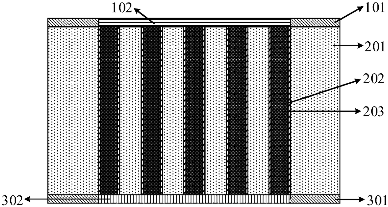
[0033] Reference figure 1 , figure 2 with image 3 The LC low-pass filter based on the silicon through hole array of the present invention includes: a top layer, a middle layer and a bottom layer.

[0034] 1. The middle layer

[0035] Reference figure 1 , figure 2 , image 3 with Figure 5 , The intermediate layer includes: a semiconductor substrate 201, an insulating layer 202 and a through silicon via metal 203.

[0036] The semiconductor substrate 201 is a silicon substrate with through-silicon vias etched through the upper and lower surfaces. The through-silicon vias are arranged in an array of 4 rows and 5 columns. In this array, the column spacing is equal to the diameter of the through-silicon vias. , The row spacing between the first row and the second row is equal to the d...


PUM


Abstract

The invention discloses a through silicon via array-based LC low-pass filter. The through silicon via array-based LC low-pass filter comprises a top layer, an intermediate layer and a bottom layer; the intermediate layer comprises a semiconductor substrate, an insulating layer and through silicon via metal; the semiconductor substrate is a silicon substrate; through silicon vias which are formed through etching and extend through the upper surface and lower surface of the semiconductor substrate are formed in the semiconductor substrate; the through silicon vias are distributed in a 4-row*5-column array structure; in the array, column spacing is equal to the diameter of the through silicon vias; the row spacing of the first row and the second row is equal to the diameter of the through silicon vias; the row spacing of the second row and the third row is equal to twice of the diameter of the through silicon vias; and the row spacing of the third row and the fourth row is equal to the diameter of the through silicon vias; and the equivalent circuit of the LC low-pass filter of the invention a 7-order LC lumped structure. The through silicon via array-based LC low-pass filter of the invention has the advantages of compact structure, high integration, small area, large inductance, flexible design and good frequency selectivity. According to the through silicon via array-based LC low-pass filter, electromagnetic radiation and coupling noises are effectively eliminated, in-band insertion loss can be effectively reduced, and out-of-band rejection can be increased.

Description

Technical field [0001] The invention relates to an LC low-pass filter, in particular to an LC low-pass filter realized based on a silicon through hole array, belonging to the field of passive devices for radio frequency / microwave integrated circuit applications. Background technique [0002] Over the past few decades, with the rapid development of the electronics industry, microwave technology has been widely used in engineering applications, and at the same time higher requirements have been put forward for the systematic integration of microwave technology. At present, microwave components are developing in the direction of miniaturization and multi-function integration. In many applications, they need to be integrated with ordinary CMOS active circuits to achieve various high-function integration system modules. However, there are Microwave components have not yet achieved this goal. [0003] As a key frequency selection device, the filter is widely used to select or limit the ...

Claims


Application Information

Patent Timeline
Patent Type & Authority Patents(China)
IPC IPC(8): H01P1/20
CPCH01P1/20
Inventor 尹湘坤朱樟明杨银堂李跃进丁瑞雪
Owner XIDIAN UNIV
Why Eureka
Try Eureka