Sensing chip
A technology for sensing chips and nanostructures, applied in measurement devices, material analysis through optical means, instruments, etc., can solve problems such as insufficient sensitivity
- Summary
- Abstract
- Description
- Claims
- Application Information
AI Technical Summary
Problems solved by technology
Method used
Image

Examples
Embodiment 1
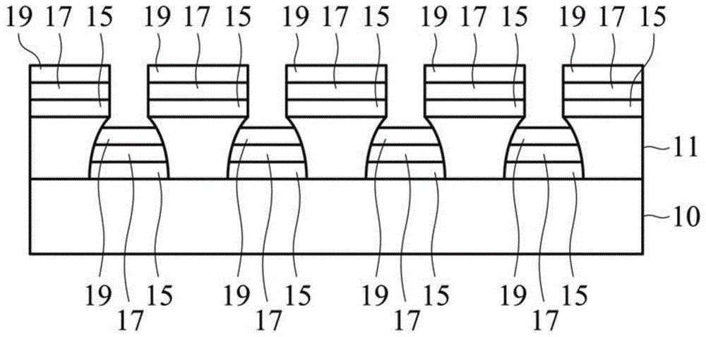
[0044] Formation of gold / alumina / gold nanostructures (MIM) on silicon oxide substrates such as Figure 5A As shown, and a single-layer gold nanostructure was formed on another silicon oxide substrate as Figure 5B Shown, and compare the distribution of the hot spots 61 of the two structures. Figure 5A In the nanostructure, the thickness of the bottom metal layer (gold) is 10nm, the thickness of the middle dielectric layer (alumina) is 20nm, and the thickness of the top metal layer (gold) is 40nm. Figure 5A The width of the nanostructure is 200nm, and the arrangement period is 650nm. Figure 5B The thickness of the monolayer gold nanostructure is 70 nm. Figure 5B The width of the nanostructure is 200nm, and the arrangement period is 650nm.
[0045] Figure 5B The hot spot of the single-layer metal nanostructure is mainly located at the junction tip of the silicon oxide substrate and the gold nanostructure. Figure 5A In addition to the distribution of the hot spot of th...
Embodiment 2
[0049] Get the MIM nanostructure of embodiment 1, adjust its period and simulate the surface plasmon resonance spectrum, such as Figure 7A shown. The simulation results show that when the period is larger, the full width at half maximum of the resonance peak is smaller. This is because when the period is larger, the surface plasmon resonance mode (LSPR mode) of the structural unit and the diffraction of the periodic structure are caused. The two conditions of Rayleigh anomaly mode are close to each other and are coupled, such as Figure 7B shown. Depend on Figure 7B It can be seen that the optimal period of the above-mentioned nanostructure is about 650 nm.
Embodiment 3
[0051] The spectral changes of the nanostructures in the two environments of air (n=1) and water (n=1.33) are as follows: Figure 8 As shown, it can be seen from the figure that the spectrum has two characteristic peaks (mode1, mode2), and the sensitivity of mode1 to the change of the environmental refractive index is higher than that of mode2. Figure 9 The thickness of the top metal layer (15nm) and bottom metal layer (15nm) of the nanostructure is fixed in air, and the thickness of the middle dielectric layer of the nanostructure is changed to confirm the influence of the thickness of the middle dielectric layer on the characteristic spectrum. It can be seen from the simulation results that the thicker the dielectric layer is, the closer the distance between the two characteristic spectra will be, and they will even overlap in the end. Conversely, when the thickness of the dielectric layer is thinner, the spectral separation is caused by the strong surface plasmon coupling ...
PUM
| Property | Measurement | Unit |
|---|---|---|
| width | aaaaa | aaaaa |
| thickness | aaaaa | aaaaa |
| thickness | aaaaa | aaaaa |
Abstract
Description
Claims
Application Information