Low-voltage trench DMOS device of high integrated level and manufacture method of device

A technology with high integration and manufacturing methods, which is applied in semiconductor/solid-state device manufacturing, semiconductor devices, electrical components, etc., can solve the problems of reducing cell size, reducing on-resistance, and insufficient registration accuracy of contact holes, etc., to achieve reduction Chip cost, increase the on-resistance per unit area, and increase the effect of cell design size

Inactive Publication Date: 2017-01-18
WUXI NCE POWER
View PDF7 Cites 2 Cited by
  • Summary
  • Abstract
  • Description
  • Claims
  • Application Information

AI Technical Summary

Problems solved by technology

[0005] The purpose of the present invention is to overcome the deficiencies in the prior art, to provide a highly integrated low-voltage trench gate DMOS device manufacturing method, on the basis of not increasing the number of photolithography, mainly to solve Trench DMOS cell design size The problem of insufficient registration accuracy of contact holes encountered during shrinkage, so as to minimize the size of the cell and reduce the on-resistance per unit area

Method used


Image

  • Low-voltage trench DMOS device of high integrated level and manufacture method of device
  • Low-voltage trench DMOS device of high integrated level and manufacture method of device
  • Low-voltage trench DMOS device of high integrated level and manufacture method of device

Examples


Embodiment 1

[0052] Embodiment 1. In this embodiment, the first conductivity type is N type, and the second conductivity type is P type;

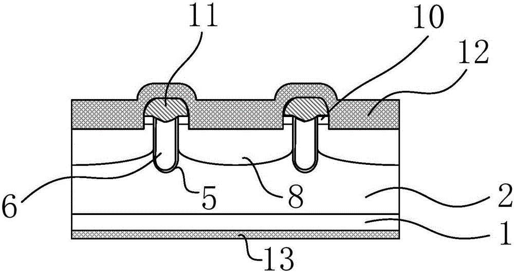
[0053] This embodiment provides a method for manufacturing a highly integrated low-voltage trench gate DMOS device, through the first insulating dielectric layer remaining above it when the gate electrode is etched, and the second insulating dielectric layer remaining on the sidewall of the gate electrode after etching back The parts together form the electrical insulation between the source metal and the gate electrode, thereby reducing the cell size and increasing the integration degree per unit area.

[0054] This method is implemented through the following steps:

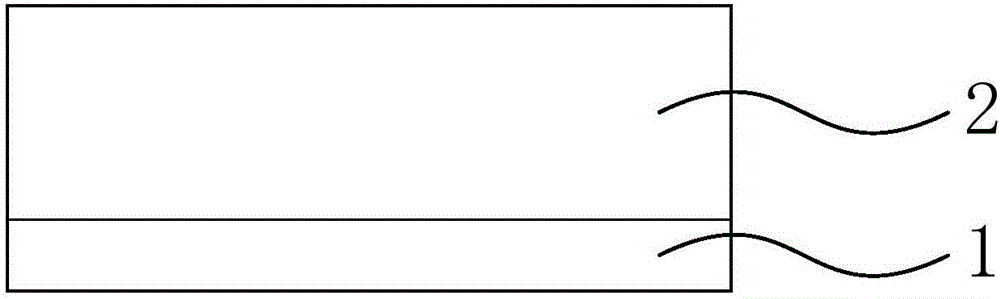
[0055] Step 1: If figure 2 As shown, an N+ type substrate 1 is provided, and an N type epitaxial layer 2 is formed on the front surface of the N+ type substrate 1;

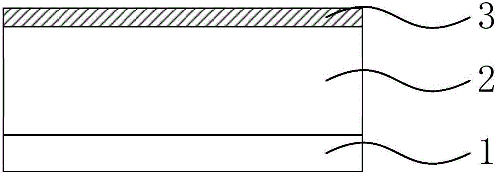
[0056] Step 2: If image 3 As shown, a trench etch barrier layer 3 is deposited on the N-type epitaxial layer 2; the ma...


PUM


Abstract

The invention provides a manufacture method of a low-voltage trench DMOS device of high integrated level. A first insulating dielectric layer is reserved over a gate electrode during etching of the gate electrode, a second insulating dielectric layer is back-etched to reserve part of the sidewall of the gate electrode, so that source electrode metal is electrically insulated from the gate electrode, the cellular size is reduced, and the integrated degree of the unit area is improved. The device and method of the invention can solve the problem that the registering precision of a contact hole is insufficient when the cellular size of Trench DMOS is reduced, the cellular size can be reduced to the largest degree, and the conducting resistance of the unit area is reduced.

Description

technical field [0001] The invention relates to the field of semiconductor integrated circuit manufacturing, in particular to a manufacturing method and structure of a highly integrated low-voltage Trench (trench gate) DMOS. Background technique [0002] At present, in semiconductor integrated circuits, the cell region structure of ordinary low-voltage Trench (trench gate) DMOS transistors is as follows: figure 1 As shown, the cell structure is mainly composed of trenches and contact holes. The contact holes form ohmic contacts by injecting high-dose dopants to lead out the body region and source region. The contact holes are dry-etched after a photolithographic exposure. Corrosion medium layer is formed. This structure is generally used in cell size designs larger than 0.9 μm. [0003] The traditional manufacturing method of low-voltage Trench DMOS is as follows: the first step: provide the first conductivity type heavily doped substrate 1, and form the first conductivit...

Claims


Application Information

Patent Timeline
Patent Type & Authority Applications(China)
IPC IPC(8): H01L29/10H01L21/336H01L29/78
CPCH01L29/1033H01L29/66674H01L29/7801
Inventor 朱袁正王根毅张硕
Owner WUXI NCE POWER
Why Eureka
Try Eureka