Multi-layer line board structure and manufacturing method thereof

A technology of multi-layer circuit and production method, applied in the direction of multi-layer circuit manufacturing, circuit substrate material, printed circuit manufacturing, etc., can solve the problems of poor circuit, excessive etching, interlayer dislocation, etc., to reduce excessive etching and improve uniformity , The effect of reducing the copper thickness range

Inactive Publication Date: 2017-01-18
KINWONG ELECTRONICS TECH LONGCHUAN
View PDF7 Cites 12 Cited by
  • Summary
  • Abstract
  • Description
  • Claims
  • Application Information

AI Technical Summary

Problems solved by technology

However, the press-fit laminated structure of multilayer circuit boards involves the superimposition of multiple materials such as inner substrates, prepregs, and copper foils, as well as production difficulties such as line width 75 μm / line spacing 75 μm, based on industry technical limitations , Problems such as misalignment between layers, dirty etching, excessive etching, and poor wiring are prone to occur during production

Method used


Image

  • Multi-layer line board structure and manufacturing method thereof
  • Multi-layer line board structure and manufacturing method thereof

Examples


Embodiment Construction

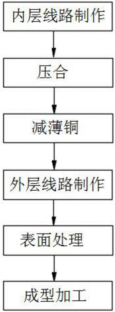
[0025] The present invention will be further described below in conjunction with the drawings and specific embodiments:

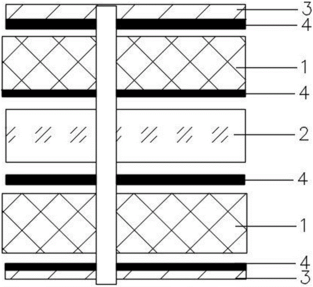
[0026] Such as figure 1 As shown, the multilayer circuit board structure of the present invention includes a plurality of inner layer substrates 1 stacked in sequence, an optical core plate 2 is arranged between adjacent inner layer substrates 1, and the upper and last layers of the first inner layer substrate 1 An outer layer of copper foil 3 is provided under an inner layer substrate 1, and a prepreg 4 is provided between the inner layer substrate 1 and the adjacent optical core board 2 or outer layer copper foil 3. The thickness of the optical core plate 2 is preferably 0.6-0.8 mm, and the thickness of the inner substrate 1 is preferably 0.1 mm. The optical core board 1 is used to replace 5 prepregs of the original technology, and the heating rate of the pressing is controlled to prevent problems such as sliding plate and interlayer dislocation during press...


PUM


Abstract

The invention relates to the multi-layer line board field and particularly relates to a multi-layer line board structure and a manufacturing method thereof. The multi-layer line board structure mainly comprises multiple inner-layer substrates which are sequentially laminated, light core boards are arranged among adjacent inner-layer substrates, outer-layer copper foils are arranged both above the first inner-layer substrate and below the last inner-layer substrate, and prepregs are respectively arranged among the inner-layer substrates and the adjacent light core boards or the outer-layer copper foils. According to the multi-layer line board structure, through combination of the light core boards and the prepregs, lamination of the multiple prepregs is reduced, and problems of board sliding and interlayer offset during stitching of the multiple prepregs are avoided. According to the method, small-current long-time electroplating technological parameters are employed, uniformity of electroplating copper thickness is improved, a copper thickness range value is reduced, and manufacturing precision of an etching line is improved; dense lines and isolate lines are designed in a segment compensation mode, line etching excess and under etching rates are reduced, and a line making qualified rate is improved.

Description

Technical field [0001] The invention relates to the field of multilayer circuit boards, in particular to a multilayer circuit board structure and a manufacturing method thereof. Background technique [0002] With the development of electronic products in the direction of high precision, high density, and high reliability, conventional mainframes, mobile phones, tablet computers and other printed circuit board mechanical through-hole products, the circuit design of line width 75μm / line spacing 75μm has become a printed circuit board. Commonly used design specifications for circuit boards. At present, improving the fine circuit process capability of multilayer circuit boards mainly depends on equipment automation solutions, such as automatic exposure machines, VCP electroplating lines, fine circuit etching machines, etc. Import high-end automatic production equipment. However, the laminated structure of multi-layer circuit boards involves multiple and multiple materials such as in...

Claims


Application Information

Patent Timeline
Patent Type & Authority Applications(China)
IPC IPC(8): H05K1/02H05K1/03H05K3/46
CPCH05K1/0298H05K1/03H05K3/4652H05K3/4655H05K2203/068H05K2203/0723
Inventor 柯勇
Owner KINWONG ELECTRONICS TECH LONGCHUAN
Why Eureka
Try Eureka