Growth method of surface passivation layer of mesa detector

A growth method and detector technology, which can be used in semiconductor devices, photovoltaic power generation, electrical components, etc., can solve the problems of increased pores at the interface, unsatisfactory passivation effect, and increased probability of pinholes, and achieve improved passivation. quality, reducing leakage current, preventing premature breakdown

Active Publication Date: 2017-01-25
THE 44TH INST OF CHINA ELECTRONICS TECH GROUP CORP
View PDF3 Cites 4 Cited by
  • Summary
  • Abstract
  • Description
  • Claims
  • Application Information

AI Technical Summary

Problems solved by technology

with monolayer SiO 2 film passivation will cause the SiO 2 The passivation layer is thinner, which leads to SiO 2 The probability of pinholes in the passivation layer increases, which can easily cause passivation to fail
Although polyimide has excellent adhesion and flow properties, when the polyimide film is directly used to passivate the mesa, the solvent is easy to volatilize when the polyimide is imidized, resulting in more pores at the interface, so the passivation The chemical effect is not ideal

Method used


Image

  • Growth method of surface passivation layer of mesa detector

Examples


Embodiment Construction

[0016] The following will clearly and completely describe the technical solutions in the embodiments of the present invention with reference to the accompanying drawings in the embodiments of the present invention. Obviously, the described embodiments are only some, not all, embodiments of the present invention. Based on the embodiments of the present invention, all other embodiments obtained by persons of ordinary skill in the art without making creative efforts belong to the protection scope of the present invention.

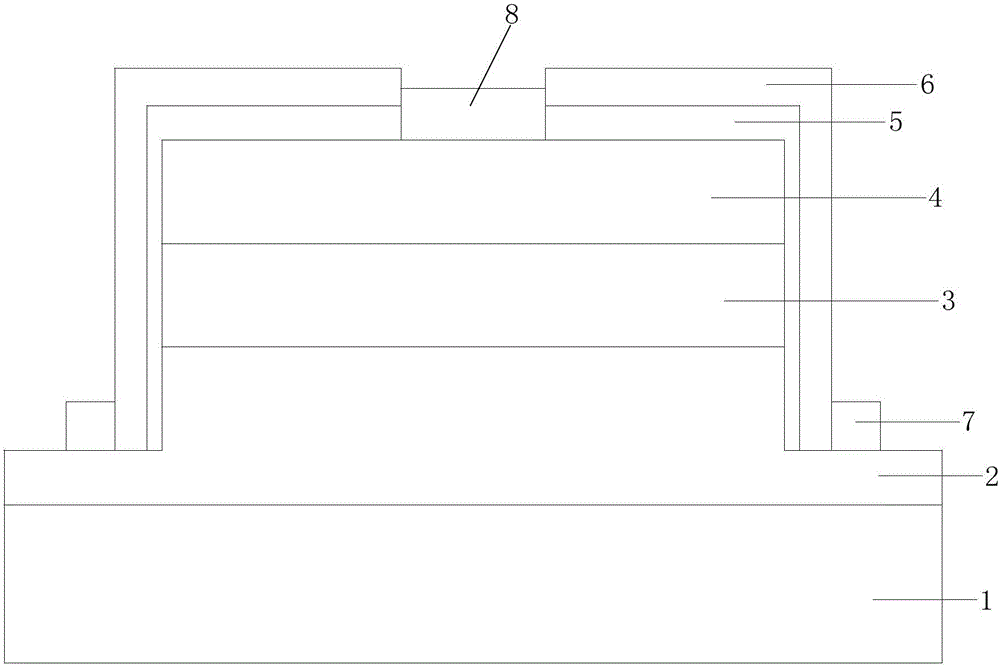
[0017] The method for growing the passivation layer on the surface of the mesa detector according to the embodiment of the present invention includes the following steps:

[0018] S1: SiO is formed on the surface of the mesa structure of the wafer using the plasma chemical vapor deposition (Plasma Enhanced Chemical Vapor Deposition, PECVD) process in a low temperature environment 2 passivation film, where SiO on the bottom and top surfaces of the mesa structur...


PUM

PropertyMeasurementUnit
thicknessaaaaaaaaaa

Abstract

The invention discloses a growth method of a surface passivation layer of a mesa detector. The growth method comprises the following steps of: forming a SiO2 passivation film on the surface of the mesa structure of a wafer by using a plasma chemical vapor deposition process in a low-temperature environment; coating a polyimide film on the SiO2 passivation film and carrying out gradient curing to densify the polyimide film; spin-coating a photoresist on the polyimide film to form a photoresist layer, and forming an exposure region on the photoresist layer; developing the photoresist layer of the exposure region, etching the polyimide film of the exposure region, and then removing the photoresist layer; performing imidization treatment on the polyimide film so that the polyimide film is fixed to the surface of the SiO2 passivation film; and etching the exposed SiO2 passivation film to set apart an electrode position. The growth method disclosed by the invention can be used for improving the passivation quality of the mesa detector, effectively reducing the surface leakage current of a device, preventing the device from premature breakdown, and improving the reliability of the device.

Description

technical field [0001] The invention relates to the field of semiconductor surface passivation, in particular to a method for growing a mesa detector surface passivation layer. Background technique [0002] The surface state is one of the key factors affecting the performance of the detector. In order to improve the performance of the device, it is necessary to reduce the surface state. Surface passivation is an effective means to suppress or reduce surface states. Compared with planar devices, the mesa detector has a larger surface area, and the PN junction around the mesa is exposed, which makes it more difficult to passivate the device surface, especially the avalanche detector (working in a high bias state). Therefore, how to improve the quality of surface passivation is the focus of attention in the development and production of mesa detectors, and is the key process of mesa detectors. If the surface passivation effect is not good, the surface of mesa detectors will be...

Claims


Application Information

Patent Timeline
Patent Type & Authority Applications(China)
IPC IPC(8): H01L31/18H01L31/101H01L31/0236
CPCY02E10/50H01L31/18H01L31/0236H01L31/101
Inventor 叶嗣荣黄俊龙赵文伯樊鹏王立
Owner THE 44TH INST OF CHINA ELECTRONICS TECH GROUP CORP
Why Eureka
Try Eureka