Control wafer recycling method

A recycling method and chemical mechanical technology, applied in electrical components, semiconductor/solid-state device manufacturing, circuits, etc., can solve the problem of uneven surface roughness, substandard particle defects on the wafer surface, uncontrollable deposition results, etc. problems, to improve the surface quality, improve the success rate of recycling, reduce the cost of production and manufacturing

Inactive Publication Date: 2017-02-01
TSINGHUA UNIV +1
View PDF3 Cites 1 Cited by
  • Summary
  • Abstract
  • Description
  • Claims
  • Application Information

AI Technical Summary

Problems solved by technology

This method, first: the deposition result is uncontrollable, the wafer has only been wet cleaned twice before depositing the silicon dioxide film, if the cleaning is not thorough enough, there will still be residual film on the surface of the wafer, or the surface of the wafer will If the unevenness and roughness are large, it will affect the deposition results, resulting in the surface particle defects of the recovered wafers not up to standard and unusable; second: some processes do not require the use of silicon dioxide or silicon nitride control chip inspection machine, so this recovery method also has limitations

Method used


Image

  • Control wafer recycling method
  • Control wafer recycling method
  • Control wafer recycling method

Examples


Embodiment Construction

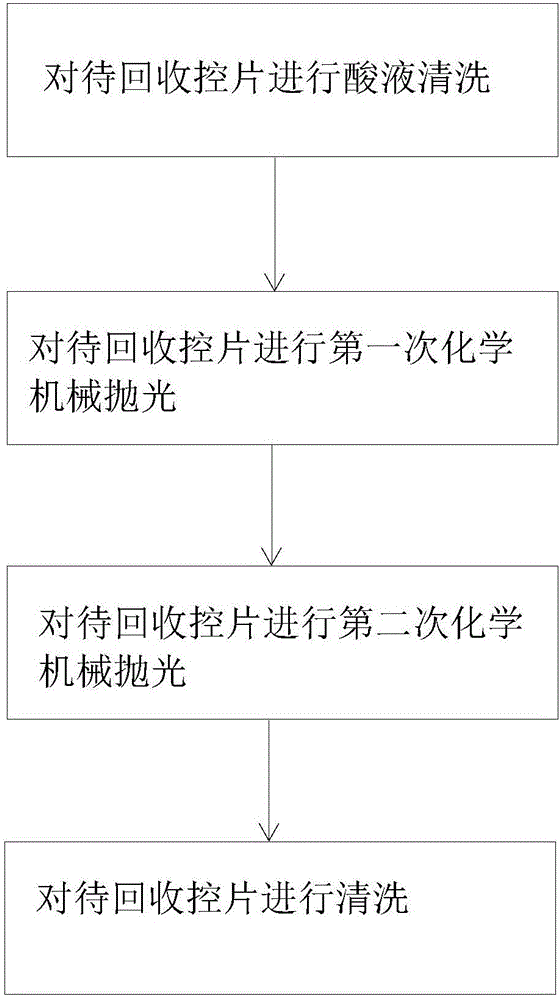
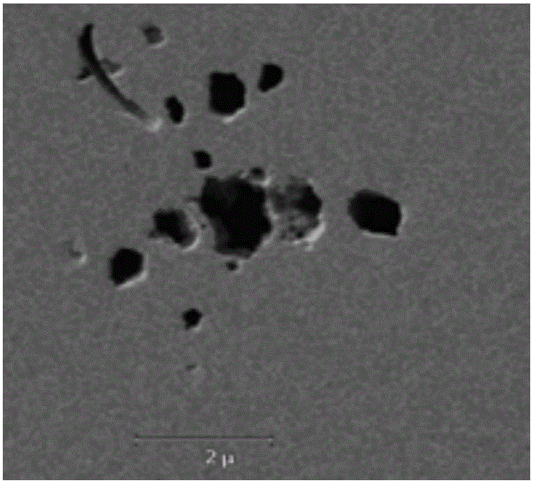
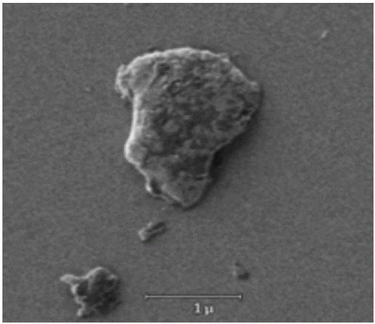
[0028] Embodiments of the invention are described in detail below, examples of which are illustrated in the accompanying drawings. The embodiments described below by referring to the figures are exemplary and are intended to explain the present invention and should not be construed as limiting the present invention.

[0029] In describing the present invention, it should be understood that the terms "center", "longitudinal", "transverse", "length", "width", "thickness", "upper", "lower", "front", " Back", "Left", "Right", "Vertical", "Horizontal", "Top", "Bottom", "Inner", "Outer", "Clockwise", "Counterclockwise", "Axial", The orientation or positional relationship indicated by "radial", "circumferential", etc. is based on the orientation or positional relationship shown in the drawings, and is only for the convenience of describing the present invention and simplifying the description, rather than indicating or implying the referred device or element Must be in a particular ...


PUM


Abstract

The invention discloses a control wafer recycling method. The control wafer recycling method comprises the following steps of performing acid liquid cleaning on a to-be-cycled control wafer; performing chemical and mechanical polishing on the to-be-cycled control wafer for the first time; and performing chemical and mechanical polishing on the to-be-cycled control wafer for the second time. According to the control wafer recycling method provided by the invention, the surface quality of the to-be-recycled control wafer is greatly improved, the recycling success rate is improved, the technological steps are simplified, and the production cost is lowered.

Description

technical field [0001] The invention relates to the field of integrated circuit manufacturing, in particular to a method for recycling control chips. Background technique [0002] The existing technical solutions usually use wet etching or cleaning methods to directly remove the coating layer on the surface of the control wafer when processing the wafers to be recycled. However, wet cleaning or acid solution immersion can only remove the surface film. If the defect If the silicon wafer below is damaged, then this method has limitations and cannot improve the success rate of control wafer recovery. [0003] In addition, there are other technical solutions that deposit a silicon dioxide or silicon nitride film on the surface of the wafer after wet cleaning, and then perform chemical mechanical polishing on the film. This method, first: the deposition result is uncontrollable, the wafer has only been wet cleaned twice before depositing the silicon dioxide film, if the cleaning...

Claims


Application Information

Patent Timeline
Patent Type & Authority Applications(China)
IPC IPC(8): H01L21/306
CPCH01L21/30625
Inventor 陈蕊王同庆李昆路新春
Owner TSINGHUA UNIV
Why Eureka
Try Eureka