QLED, manufacturing method therefor and illuminating device
A quantum dot light-emitting and insulating layer technology, applied in semiconductor/solid-state device manufacturing, electrical components, electrical solid-state devices, etc., can solve the problem that the performance of QLED needs to be improved, and achieve the effect of increasing the recombination probability and improving the overall efficiency.
- Summary
- Abstract
- Description
- Claims
- Application Information
AI Technical Summary
Problems solved by technology
Method used
Image

Examples
Embodiment 1
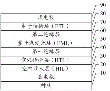
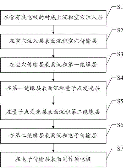
[0059] 1) The glass substrate containing ITO (120nm) was subjected to cleaning agent, acetone, IPA (isopropanol) and deionized water for 15 minutes, then dried, and treated with ozone plasma for 10 minutes;
[0060] 2) Depositing a hole injection layer on the glass substrate, the material of the hole injection layer is PEDOT:PSS (thickness 40nm), and then heating at 150°C for 15 minutes;
[0061] 3) Deposit a hole transport layer on the hole injection layer. The material of the hole transport layer is TFB with a thickness of 25nm. Specifically, it is spin-coated in a glove box to form a film, and then heated at 150°C for 30 minute;
[0062] 4) Depositing a first insulating layer on the hole transport layer, the material of the first insulating layer is PMMA, the thickness is 5nm, the solvent is acetone solution, and heated at 50°C for 10 minutes after film formation;
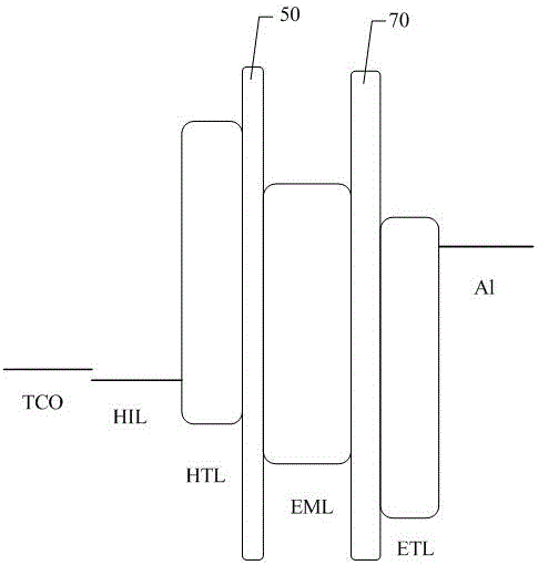
[0063] 5) Deposit a quantum dot light-emitting layer on the first insulating layer, the material of the quan...
Embodiment 2
[0068] 1) The glass substrate containing ITO (120nm) was subjected to cleaning agent, acetone, IPA (isopropanol) and deionized water for 15 minutes, then dried, and treated with ozone plasma for 10 minutes;
[0069] 2) Depositing a hole injection layer on the glass substrate, the material of the hole injection layer is PEDOT:PSS (thickness 40nm), and then heating at 150°C for 15 minutes;
[0070] 3) Deposit a hole transport layer on the hole injection layer. The material of the hole transport layer is TFB with a thickness of 25nm. Specifically, it is spin-coated in a glove box to form a film, and then heated at 150°C for 30 minute;
[0071] 4) Depositing a first insulating layer on the hole transport layer, the material of the first insulating layer is SiO 2 , the thickness is 5nm, the sol solution is spin-coated to form a film, and heated at 150°C for 30 minutes after the film is formed;
[0072] 5) Deposit a quantum dot light-emitting layer on the first insulating layer, t...
Embodiment 3
[0077] 1) The glass substrate containing ITO (120nm) was subjected to cleaning agent, acetone, IPA (isopropanol) and deionized water for 15 minutes, then dried, and treated with ozone plasma for 10 minutes;
[0078] 2) Depositing a hole injection layer on the glass substrate, the material of the hole injection layer is PEDOT:PSS (thickness 40nm), and then heating at 150°C for 15 minutes;
[0079] 3) Deposit a hole transport layer on the hole injection layer. The material of the hole transport layer is TFB with a thickness of 25nm. Specifically, it is spin-coated in a glove box to form a film, and then heated at 150°C for 30 minute;
[0080] 4) Depositing a first insulating layer on the hole transport layer, the material of the first insulating layer is PMMA, the thickness is 8nm, the solvent is acetone solution, and heated at 50°C for 10 minutes after film formation;
[0081] 5) Depositing a quantum dot light-emitting layer on the first insulating layer, the material of the q...
PUM
 Abstract
Description
Claims
Application Information
PatSnap Eureka turns technology decisions into work you can execute. Powered by our Innovation Knowledge Graph, it runs expert workflows across engineering, life sciences, materials and intellectual property. Get your review-ready output in minutes.


