Nano-pillar LED grown on strontium tantalum lanthanum aluminate substrate and preparation method thereof

A technology of strontium tantalum lanthanum aluminate and nano-pillars, applied in electrical components, circuits, semiconductor devices and other directions, can solve problems such as unstable chemical properties of substrates, and achieve the effects of eliminating adverse effects, reducing growth difficulty, and reducing production costs.

Active Publication Date: 2017-02-08
SOUTH CHINA UNIV OF TECH
View PDF7 Cites 6 Cited by
  • Summary
  • Abstract
  • Description
  • Claims
  • Application Information

AI Technical Summary

Problems solved by technology

But La 0.3 Sr 1.7 AlTaO 6 The chemical properties of the substrate are unstable at high temperature, so it is necessary to make La 0.3 Sr 1.7 AlTaO 6 On-substrate nanoc

Method used


Image

  • Nano-pillar LED grown on strontium tantalum lanthanum aluminate substrate and preparation method thereof
  • Nano-pillar LED grown on strontium tantalum lanthanum aluminate substrate and preparation method thereof
  • Nano-pillar LED grown on strontium tantalum lanthanum aluminate substrate and preparation method thereof

Examples


Embodiment 1

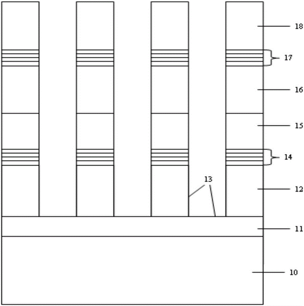
[0049] The preparation method of the nanocolumn LED grown on the strontium tantalum lanthanum aluminate substrate of this embodiment comprises the following steps:

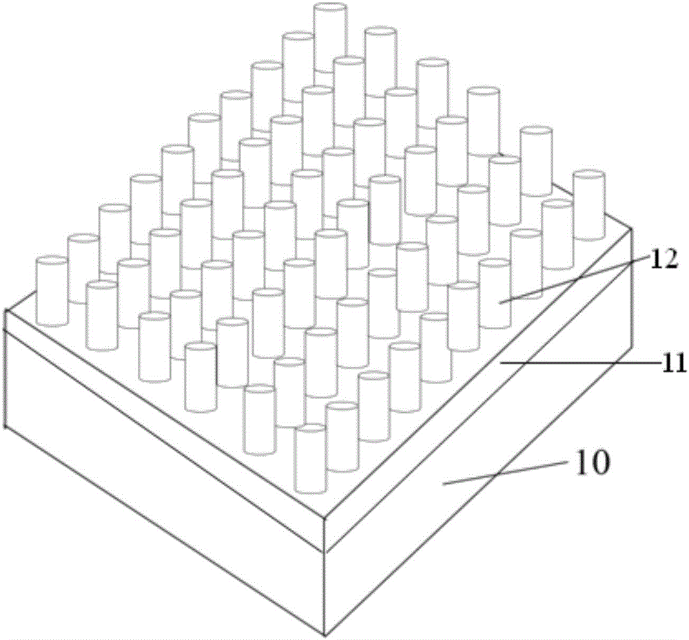
[0050] (1) Selection of the substrate and its crystal orientation: using La 0.3 Sr 1.7 AlTaO 6 The substrate, with the (111) plane offset from the (100) direction by 0.5-1° as the epitaxial plane, the crystal epitaxial orientation relationship is: the (0001) plane of GaN is parallel to the La 0.3 Sr 1.7 AlTaO 6 (111) side;

[0051] (2) Substrate surface polishing, cleaning and annealing treatment, the specific process of the annealing is: put the substrate into the annealing chamber, and treat La 0.3 Sr 1.7 AlTaO 6 The substrate was annealed for 3 hours and then air-cooled to room temperature;

[0052] The surface polishing of the substrate is specifically: firstly La 0.3 Sr 1.7 AlTaO 6 The surface of the substrate is polished with diamond slurry, and the surface of the substrate is observed with an opt...

Embodiment 2

[0066] The preparation method of the nanocolumn LED grown on the strontium tantalum lanthanum aluminate substrate of this embodiment comprises the following steps:

[0067] (1) Selection of the substrate and its crystal orientation: using La 0.3 Sr 1.7 AlTaO 6 The substrate, with the (111) plane offset from the (100) direction by 0.5-1° as the epitaxial plane, the crystal epitaxial orientation relationship is: the (0001) plane of GaN is parallel to the La 0.3 Sr 1.7 AlTaO 6 (111) side;

[0068] (2) Substrate surface polishing, cleaning and annealing treatment, the specific process of the annealing is: put the substrate into the annealing chamber, and treat La 0.3 Sr 1.7 AlTaO 6 The substrate was annealed for 5 hours and then air-cooled to room temperature;

[0069] The surface polishing of the substrate is specifically: firstly La 0.3 Sr 1.7 AlTaO 6 The surface of the substrate is polished with diamond slurry, and the surface of the substrate is observed with an opt...


PUM

PropertyMeasurementUnit
Heightaaaaaaaaaa
Diameteraaaaaaaaaa
Thicknessaaaaaaaaaa

Abstract

The invention belongs to the technical field of nano-pillar LED preparation, and discloses a nano-pillar LED grown on a strontium tantalum lanthanum aluminate substrate and a preparation method thereof. The nano-pillar LED grown on a strontium tantalum lanthanum aluminate substrate comprises a strontium tantalum lanthanum aluminate substrate, an AlN nucleation layer grown on the strontium tantalum lanthanum aluminate substrate, a GaN nano-pillar template grown on the AlN nucleation layer, an AlN/GaN super lattice layer grown on the GaN nano-pillar template, a non-doped GaN layer grown on the AlN/GaN super lattice layer, an n-type doped GaN layer grown on the non-doped GaN layer, an InGaN/GaN quantum well grown on the n-type doped GaN layer, and a p-type doped GaN layer grown on the InGaN/GaN quantum well. The substrate material is of low cost. A nano-pillar array prepared is size-controllable and of uniform orientation. The obtained nano-pillar LED has low defect density and excellent electrical and optical properties.

Description

technical field [0001] The invention relates to the field of growth and preparation of nano-array LEDs, in particular to the field of growth on strontium aluminate tantalum lanthanum (La 0.3 Sr 1.7 AlTaO 6 ) nanocolumn LED on the substrate and its preparation method. Background technique [0002] GaN and its related group III nitrides have excellent electrical, optical, and acoustic properties, and have been widely used in the preparation of light-emitting diodes (LEDs), laser diodes (LDs), and field-effect transistors. In recent years, GaN-based nanopillar LEDs have attracted much attention as a potential LED structure. Compared with planar LEDs, nanopillar LEDs have a high surface-to-volume ratio (area / volume), which can significantly reduce wear and tear. Dislocation density; secondly, nano-column LEDs can greatly improve the light-emitting efficiency of LEDs and realize light coupling and output; finally, by controlling the size of nano-column LEDs and changing the li...

Claims


Application Information

Patent Timeline
IPC IPC(8): H01L33/02H01L33/06H01L33/12H01L33/00
CPCH01L33/007H01L33/02H01L33/06H01L33/12
Inventor 李国强王文樑杨美娟
Owner SOUTH CHINA UNIV OF TECH
Why Eureka
Try Eureka