Frequency band scanning circuit for LC type phase locked loop
A scanning circuit and phase-locked loop technology, applied in the field of microelectronics, can solve the problems of complicated calculation process and configuration, and achieve the effect of simplifying the frequency band calculation process and circuit configuration
- Summary
- Abstract
- Description
- Claims
- Application Information
AI Technical Summary
Problems solved by technology
Method used
Image

Examples
Embodiment Construction
[0016] The specific implementation manners of the present invention will be described below in conjunction with the accompanying drawings and specific examples.
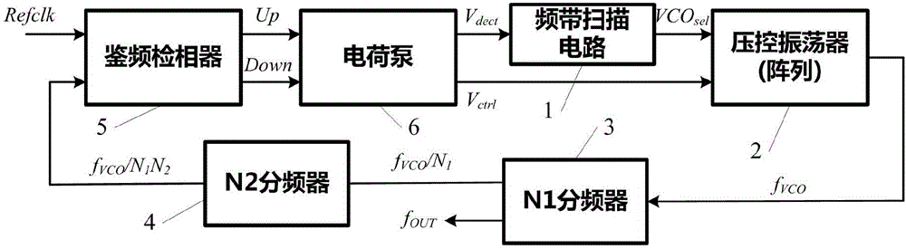
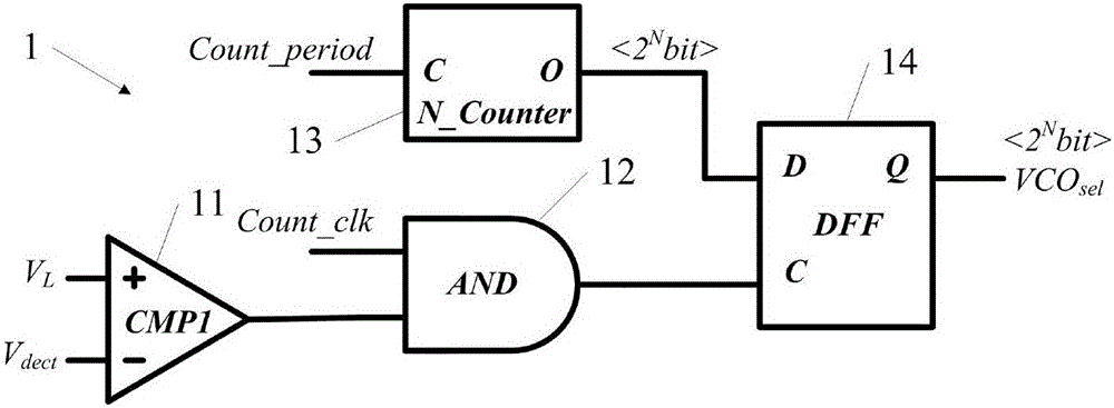
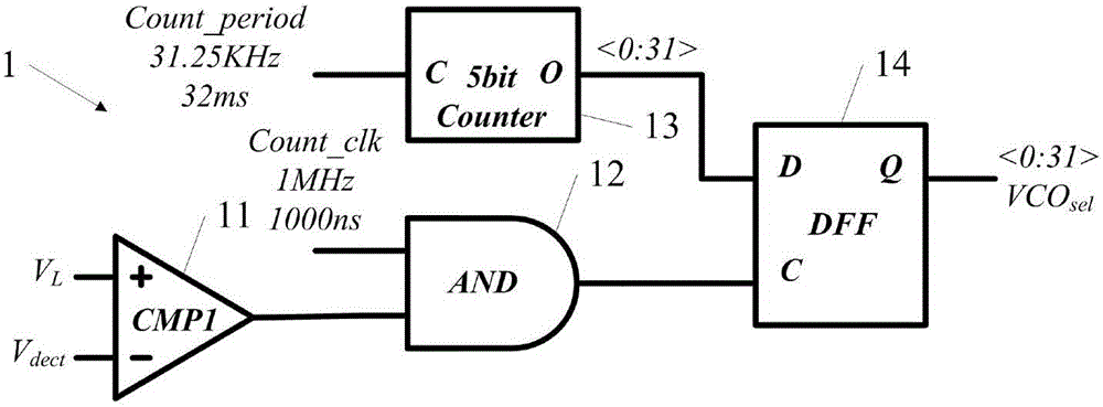
[0017] figure 1 It is the schematic diagram of the LC-type phase-locked loop circuit used in the actual implementation of the present invention. This circuit is a typical LC-type phase-locked loop. The voltage-controlled oscillator 2 adopts a 32-segment array structure such as Figure 4 As shown, the output of the voltage-controlled oscillator 2 is divided twice by the N1 frequency divider 3 and the N2 frequency divider 4 and then provided to the frequency discrimination and phase detector PFD 5 for frequency discrimination and phase detection with the input reference clock Refclk. The frequency band scanning circuit 1 is located between the charge pump 6 and the voltage-controlled oscillator 2, and the voltage V is determined by comparison dect Get the 32-bit selection signal VCO set Used to control the VCO 2 arra...
PUM
 Abstract
Description
Claims
Application Information
 - R&D
- Intellectual Property
- Life Sciences
- Materials
- Tech Scout
- Unparalleled Data Quality
- Higher Quality Content
- 60% Fewer Hallucinations
Browse by: Latest US Patents, China's latest patents, Technical Efficacy Thesaurus, Application Domain, Technology Topic, Popular Technical Reports.
© 2025 PatSnap. All rights reserved.Legal|Privacy policy|Modern Slavery Act Transparency Statement|Sitemap|About US| Contact US: help@patsnap.com