Customizable high-gain ZnO nanowire array UV detector and preparation method thereof
A nanowire array and ultraviolet detector technology, which is applied in the field of nanotechnology and ultraviolet detection, can solve the problems of high cost, long cycle, and affecting the overall area of the device, and achieve the effect of solving the problem of controllability of the growth direction and high uniformity
- Summary
- Abstract
- Description
- Claims
- Application Information
AI Technical Summary
Problems solved by technology
Method used
Image
Examples
Embodiment 1
[0033] The invention is a custom-made high-gain ZnO nanowire array ultraviolet detection device, specifically a method for detecting ultraviolet light by detecting the change of the conductivity of the ZnO nanowire.
[0034]The specific structure of a customized high-gain ZnO nanowire array ultraviolet detection device disclosed in the present invention is as follows:
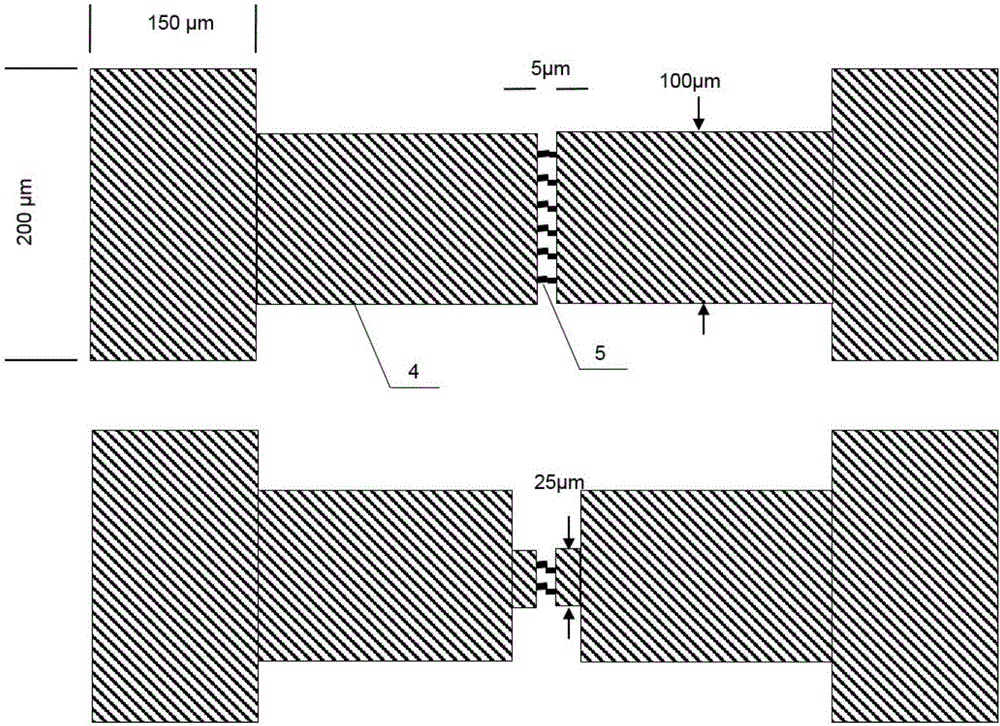
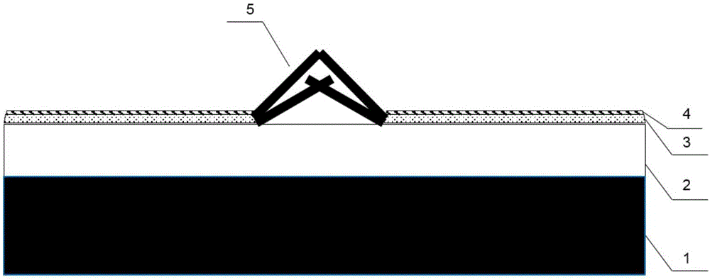
[0035] There are two completely symmetrical electrodes on the surface of the Si substrate, each part of the electrode is composed of a 200 micron*100 micron rectangle and a 150 micron*200 micron rectangular connection, and the distance between the two electrodes is 5 microns. The components of all patterns are: 100nm ZnO seed layer and 115nm Ti / Au electrodes.
[0036] For the ultraviolet detection device, the Si substrate is selected as the substrate of the present invention. In order to ensure that there is no mutual influence between the devices, the SiO substrate of 300nm is selected to be grown. 2 Insulati...
Embodiment 2
[0044] The same electrode pattern structure as in Example 1, there are two completely symmetrical electrodes on the surface of the Si substrate, each part of the electrode is composed of a 200 micron*100 micron rectangle connected with a 150 micron*200 micron rectangle, and the distance between the two electrodes is 5 Microns. The components of all patterns are: 50nm ZnO seed layer and 115nm Ti / Au electrodes.
[0045] For the ultraviolet detection device, the Si substrate is selected as the substrate of the present invention. In order to ensure that there is no mutual influence between the devices, the SiO substrate of 300nm is selected to be grown. 2 Insulation. After making electrodes on the side and surface of the steps, ZnO nanowires are grown laterally. Its specific preparation method is as follows:
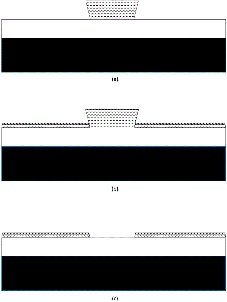
[0046] (1) First, after pre-baking the above-mentioned Si-based substrate, spin-coat AZ-5214 photoresist with a thickness of 1.5 microns. Engraved on the surface of the ...
PUM
| Property | Measurement | Unit |
|---|---|---|
| thickness | aaaaa | aaaaa |
| width | aaaaa | aaaaa |
| length | aaaaa | aaaaa |
Abstract
Description
Claims
Application Information


