
Current feedback type instrument amplifier with low power consumption and low noise
An instrumentation amplifier, current feedback technology, applied in amplifiers, DC-coupled DC amplifiers, differential amplifiers, etc., can solve the problems of high noise and high power consumption, achieve chip area reduction, small chip area and cost, reduce power consumption and effect of noise
- Summary
- Abstract
- Description
- Claims
- Application Information
AI Technical Summary
Problems solved by technology
Method used
Image

Examples
Embodiment Construction
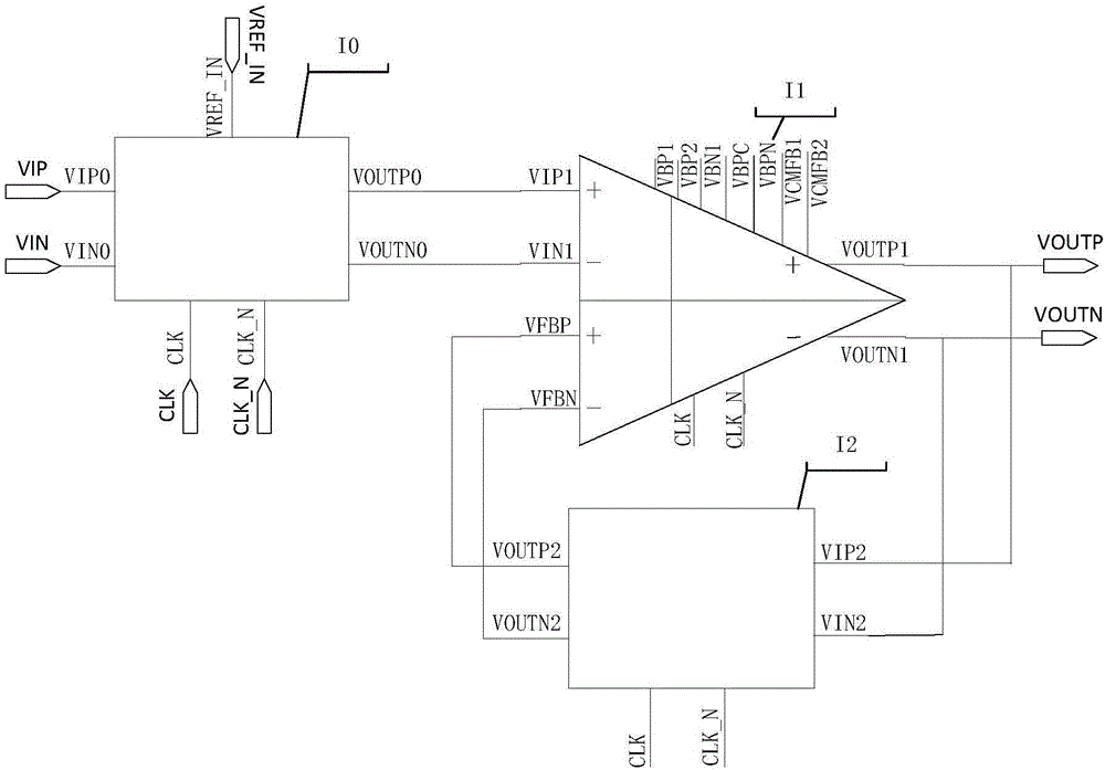
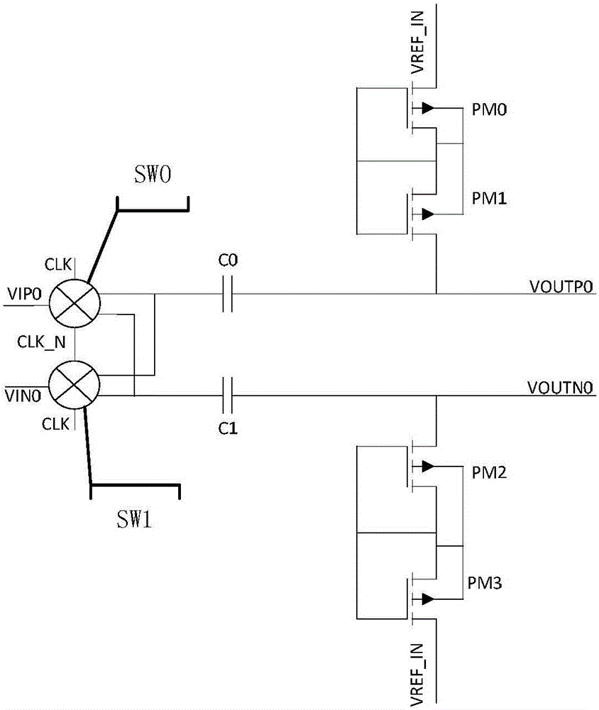
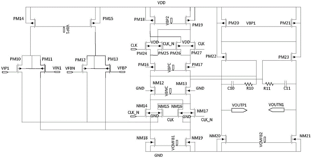
[0020] A low-power, low-noise current-feedback instrumentation amplifier, such as figure 1 As shown, it includes input preprocessing circuit I0, operational transconductance amplification (OTA) circuit and capacitive feedback network I2. The non-inverting input terminal VIP0 of the input pre-processing circuit I0 forms the non-inverting input terminal VIP of the amplifier, and the inverting input terminal VIN0 of the input pre-processing circuit I0 forms the inverting input terminal VIN of the amplifier. The differential in-phase output terminal VOUTP0 of the input preprocessing circuit I0 is connected to the in-phase differential input terminal VIP1 of the OTA circuit I1. The differential inverting output terminal VOUTN0 of the input preprocessing circuit I0 is connected to the inverting differential input terminal VIN1 of the OTA circuit I1. The non-inverting feedback input terminal VFBP of the OTA circuit I1 is connected to the non-inverting output terminal VOUTP2 of the c...
PUM
 Abstract
Description
Claims
Application Information