Printed circuit board resin laminate for forming fine via hole, and multilayer printed circuit board having fine via hole in resin insulating layer and method for manufacturing same

A laminated body and insulating layer technology, applied in the direction of printed circuit manufacturing, printed circuit, printed circuit components, etc., can solve the problem of not involving via holes, etc., and achieve the effect of high conductive reliability

Inactive Publication Date: 2017-02-15
MITSUBISHI GAS CHEM CO INC
View PDF9 Cites 1 Cited by
  • Summary
  • Abstract
  • Description
  • Claims
  • Application Information

AI Technical Summary

Problems solved by technology

Therefore, these documents do not refer to the formation of fine via holes having a top diameter of 30 μm or less.

Method used


Image

  • Printed circuit board resin laminate for forming fine via hole, and multilayer printed circuit board having fine via hole in resin insulating layer and method for manufacturing same
  • Printed circuit board resin laminate for forming fine via hole, and multilayer printed circuit board having fine via hole in resin insulating layer and method for manufacturing same
  • Printed circuit board resin laminate for forming fine via hole, and multilayer printed circuit board having fine via hole in resin insulating layer and method for manufacturing same

Examples


Embodiment

[0138] [Manufacture of cyanate compounds]

Synthetic example 1

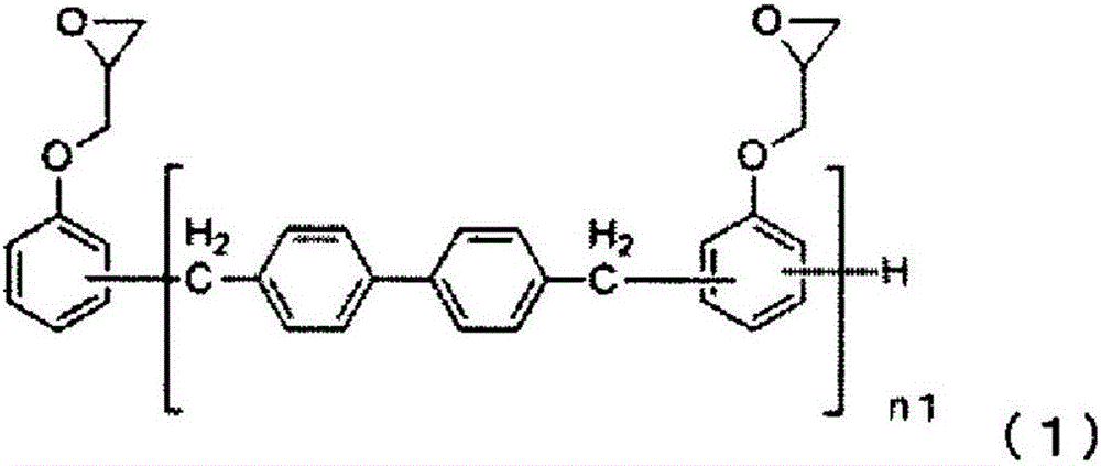
[0139] The synthesis of synthetic example 1α-naphthol aralkyl type cyanate compound (the compound of formula (8):

[0140]

[0141] (In the formula, the average value of n is 3-4.)

[0142] The reactor equipped with thermometer, stirrer, dropping funnel and reflux condenser is pre-cooled to 0-5°C with salt water, and 7.47g (0.122mol) of cyanogen chloride and 9.75g (0.0935mol) of 35% hydrochloric acid are put into it. ), water 76ml and dichloromethane 44ml.

[0143] While keeping the temperature in the reactor at -5 to +5°C and the pH at 1 or less, add the following formula (8') dropwise to 92 ml of dichloromethane through the dropping funnel over 1 hour under stirring. 20 g (0.0935 mol) of the indicated α-naphthol aralkyl resin (SN485, OH group equivalent: 214 g / eq. softening point: 86° C., manufactured by Nippon Steel Chemical Co., Ltd.) and triethylamine 14.16 g ( 0.14 mol) solution, after the dropwise addition was completed, 4.72 g (0.047 mol) of triethylamine was furt...

Embodiment 1

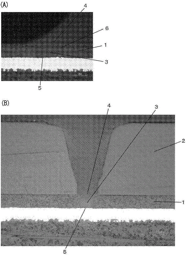
[0155] Example 1: Use of a PET film with a release layer with a total thickness of 75 μm

[0156] As a release film for laser attenuation, a PET film with a release layer having a total thickness of 75 μm was used, and the resin composition layer after drying was uniformly coated so that the thickness of the resin composition layer became 20 μm, using the column of Example 1 in Table 1. The stated machining energy is used to open holes.


PUM

PropertyMeasurementUnit
thicknessaaaaaaaaaa
thicknessaaaaaaaaaa
thicknessaaaaaaaaaa

Abstract

Provided is a method for processing or manufacturing a printed circuit board in which it is possible to form a via hole in which the top diameter is reduced and the difference between the top diameter and the bottom diameter is smaller. Also provided is a resin laminate used in this method. A printed wiring board resin laminate including a resin insulating layer for forming a fine via hole and a release film for laser attenuation laminated on the resin insulating layer, wherein the thickness of the release film for laser attenuation is set to over 50 [mu]m and no more than 180 [mu]m, making it possible to form a via hole having a top diameter of 30 [mu]m or less and a difference between the top diameter and the bottom diameter of 10 [mu]m or less.

Description

technical field [0001] The present invention relates to a resin laminate for a printed wiring board for forming fine via holes, a multilayer printed wiring board having fine via holes in a resin insulating layer, and a manufacturing method thereof. Background technique [0002] In recent years, the miniaturization and high performance of electronic equipment have been promoted, and for multilayer printed circuit boards, in order to increase the mounting density of electronic components and the miniaturization of conductor wiring has been promoted, the wiring formation technology is expected. As a method of forming high-density fine wiring on the insulating layer, there are known: an additive method of forming a conductor layer only by electroless plating; forming a thin copper layer on the entire surface by electroless plating, and then forming a conductor layer by electrolytic plating, Then the thin copper layer is subjected to a semi-additive method of rapid etching, etc. ...

Claims


Application Information

Patent Timeline
Patent Type & Authority Applications(China)
IPC IPC(8): H05K3/00B23K26/382B32B27/00B32B27/36H05K1/03H05K3/46
CPCB23K26/382B32B27/00B32B27/36H05K1/03H05K3/00H05K3/46B32B27/08B32B27/20B32B27/38B32B2307/206B32B2457/08H05K1/0313H05K3/0026H05K3/429H05K3/4655
Inventor 铃木卓也
Owner MITSUBISHI GAS CHEM CO INC
Why Eureka
Try Eureka