Stack type single base island SIP (System in Package) packaging process

A packaging technology and stacking technology, which is applied in the manufacture of electrical components, electrical solid devices, semiconductor/solid devices, etc., can solve the problems of MOS chip size that cannot be attached, overheating damage, and poor heat dissipation in the packaging form, so as to avoid the formation of creeping Electric phenomena, enlarging the package size, and taking up less space

Active Publication Date: 2017-02-22
华蓥旗邦微电子有限公司
View PDF5 Cites 3 Cited by
  • Summary
  • Abstract
  • Description
  • Claims
  • Application Information

AI Technical Summary

Problems solved by technology

However, as the power of mobile phone chargers is getting larger and larger, the existing technology can no longer meet the needs in the field of mobile phone chargers with increasingly fast charging and high power, and LED control due to the use of the original packaging form:
[0003] 1. After high power, the original packaging form has poor heat dissipation. At present, the SOP series can only achieve 7-8W, and the DIP series can only achieve about 7-15W. If the power is too large, it is easy to cause overheating damage;
[0004] 2. After the power is increased, the area of ​​the MOS chip will also increase. Since the original packaging form adopts the horizontal arrangement of double-base islands, the size of the high-power MOS chip cannot be attached to the existing package frame base island.

Method used


Image

  • Stack type single base island SIP (System in Package) packaging process
  • Stack type single base island SIP (System in Package) packaging process
  • Stack type single base island SIP (System in Package) packaging process

Examples


Embodiment Construction

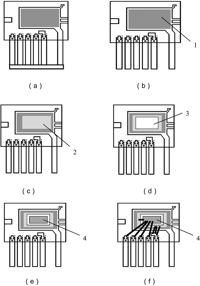
[0028] refer to Figure 1-3 , a stacked single-substrate island SIP packaging process of the present invention, comprising the following steps:

[0029] Step 1, take a frame with a single base island;

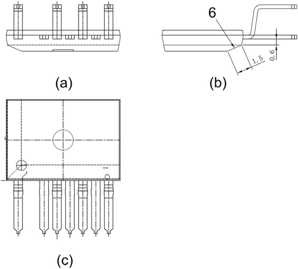
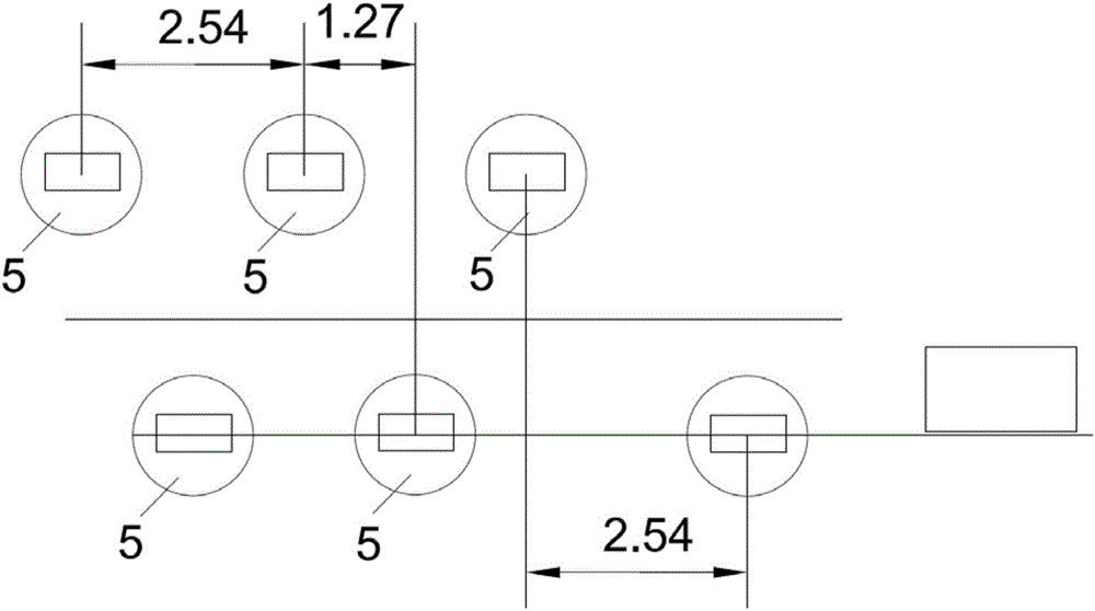
[0030] Step 2, step 2, weld the pin group on the frame, the pin group includes several chip pin groups for connecting the chip, the chip pin group includes several chip pin groups with an interval of 1.27mm and is arranged side by side Chip pin 5, cut off the pin connection end, and then bend the chip pins 5 in odd or even rows in the chip pin group horizontally to form two columns of pins with an interval of 2.54mm to form a lead frame;

[0031] Step 3, spot soft solder 1 on the single base island of the lead frame;

[0032] Step 4: Paste the first chip 2 on the single base island with soft solder 1 on it, and then heat to 260-300°C to melt the soft solder 1 to weld the first chip 2 and the lead frame together;

[0033] Step five, point insulating glue 3 on the surface of t...


PUM


Abstract

The invention discloses a stack type single-base island SIP (System in Package) packaging process. The process comprises the following steps: step I, taking a frame with a single base island; step II, welding a pin group on the frame, and cutting pin connection ends to form a lead frame; step III, dispensing a soft weld material on the single base island of the lead frame; step IV, pasting a first chip to the single base island with the soft weld material, and heating to melt the soft weld material so as to weld the first chip with the lead frame; step V, dispersing insulating glue to the surface of the first chip; step VI, pasting a second chip to the surface of the first chip, and bonding the second chip with the first chip through the insulating glue; step VII, connecting the first chip with the second chip through a metal line, connecting the first chip with the pins, and connecting the second chip with the pins; and step VIII, completing later procedures of packaging, cleaning and cutting. By adopting the stack type single system in package SIP packaging process disclosed by the invention, the heat radiation property of an integrated circuit can be improved, and the problem that a large space can be occupied by a power supply management chip can be solved.

Description

technical field [0001] The invention belongs to the technical field of semiconductor packaging, and in particular relates to a stacked single-base island SIP packaging process, which is mainly applied to intelligent control integrated circuits used in mobile phone chargers and LED constant-current power supplies. Background technique [0002] At present, the packaging forms of intelligent control integrated circuits used in mobile phone chargers and LED constant current power supplies are DIP8L, DIP7L, SOP8L, SOP7L, etc. Paste the MOS chip. However, as the power of mobile phone chargers is getting larger and larger, the existing technology can no longer meet the needs in the field of mobile phone chargers with increasingly fast charging and high power, and LED control due to the use of the original packaging form: [0003] 1. After high power, the original packaging form has poor heat dissipation. At present, the SOP series can only achieve 7-8W, and the DIP series can only...

Claims


Application Information

Patent Timeline
Patent Type & Authority Applications(China)
IPC IPC(8): H01L21/768H01L23/495H01L23/538
CPCH01L2224/48247H01L2924/19107H01L23/538H01L21/768H01L23/49534
Inventor 邓云卫
Owner 华蓥旗邦微电子有限公司
Why Eureka
Try Eureka