SiC-based groove-type field effect transistor and preparation method thereof

A field-effect transistor, trench-type technology, applied in the field of SiC-based UMOSFET fabrication, can solve problems such as unfavorable breakdown voltage, device breakdown, and low channel mobility, and achieve improved on-state conductivity and dynamic switching loss. The effect of reducing and avoiding JFET resistance

Active Publication Date: 2017-02-22
ZHEJIANG XINKE SEMICON CO LTD
View PDF2 Cites 13 Cited by
  • Summary
  • Abstract
  • Description
  • Claims
  • Application Information

AI Technical Summary

Problems solved by technology

[0003] However, on the one hand, the high gate-oxygen interface state density of SiC-based MOS devices leads to low channel mobility, which has always restricted the improvement of the on-state performance of MOSFET devices; on the other hand, under high reverse voltage, the trench oxidation The electric field in the object is too large, especially the two-dimensional electric field accumulation at the corner of the bottom groove, which causes device breakdown in advance, which is not conducive to the improvement of the breakdown voltage; although a series of measures are taken, such as injecting a p-type shielding layer at the bottom of the groove to protect the electric field of the oxide layer , but the JFET resistance brought by it is not conducive to the improvement of the on-state characteristics of 4H-SiC-based trench MOSFET (UMOSFET)

Method used


Image

  • SiC-based groove-type field effect transistor and preparation method thereof
  • SiC-based groove-type field effect transistor and preparation method thereof
  • SiC-based groove-type field effect transistor and preparation method thereof

Examples


Embodiment Construction

[0033] In order to make the object, technical solution and advantages of the present invention clearer, the present invention will be further described in detail below in conjunction with specific embodiments and with reference to the accompanying drawings.

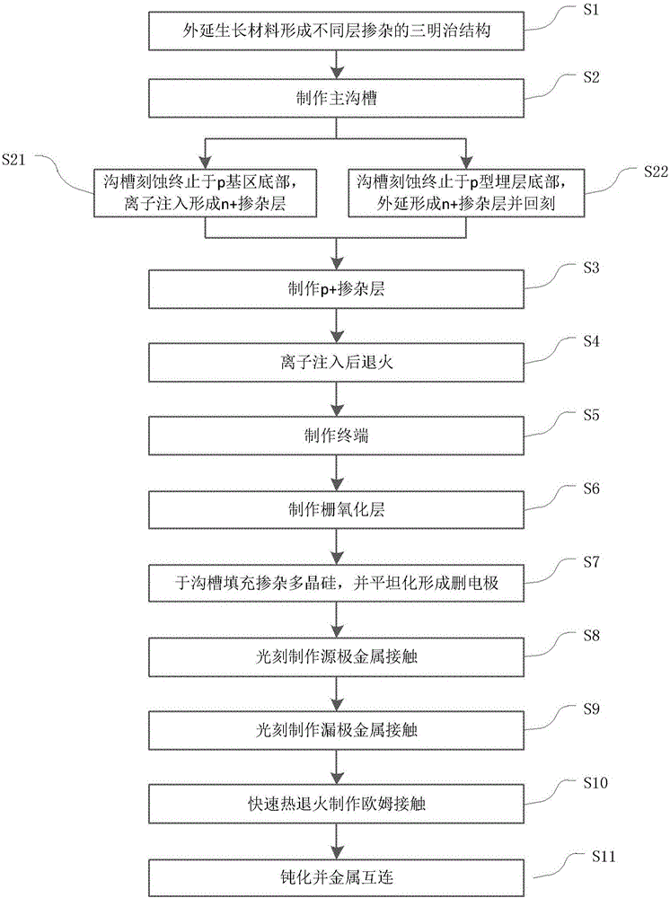
[0034] figure 1 A process flow for preparing a SiC-based UMOSFET according to an embodiment of the present invention is shown, including the following steps:

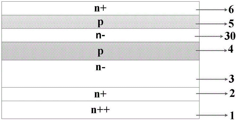
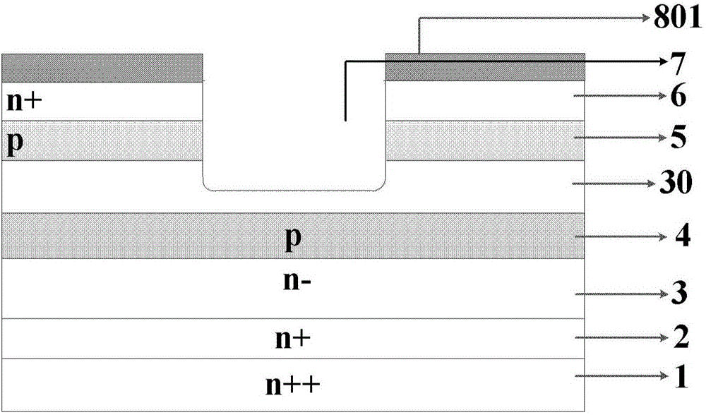
[0035] In step S1, the epitaxial growth material forms a sandwich structure doped in different layers. According to an embodiment of the present invention, such as figure 2 As shown, using chemical vapor deposition or other methods of epitaxial growth materials to epitaxially grow multiple layers of SiC epitaxial layers of different doping types on the SiC n++ type substrate substrate 1, forming a sandwich structure, from bottom to top in order: : n+ type buffer layer 2, n-drift layer 3, p-type buried layer 4, n-drift layer 30, p-type base region layer 5, n+ sou...


PUM


Abstract

The invention discloses a preparation method of a bottom n-type doped SiC-based UMOSFET with a p-type buried layer and a groove. The method is characterized in that the p-type buried layer (4) is formed through epitaxial growth on an n- drift layer (3); an n- drift layer (30) is formed through epitaxial growth on the p-type buried layer (4); a p-type base region layer (5) is formed through epitaxial growth on the n- drift layer (30); and an n-type doped layer (900) is formed at the bottom of a main groove (7). The electric field of a gate oxide layer (10) is effectively reduced in a reverse blocking state. Due to the shielding effects of the p-type buried layer (4) and the n-type doped layer (900), the thickness of the p-type base region layer (5) is greatly reduced, the groove is reduced to below 0.5[mu]m and the on-state performance is improved. The SiC-based UMOSFET has a relatively high Baliga optimum value and a relatively low switching loss. The invention further provides a structure of the SiC-based UMOSFET.

Description

technical field [0001] The invention relates to a method for preparing a SiC-based trench field effect transistor (MOSFET), in particular to a method for manufacturing a SiC-based UMOSFET with a p-type buried layer and n-type doping at the bottom of the trench. Background technique [0002] SiC has superior physical and electrical properties, such as high critical breakdown electric field, wide band gap, and high electron saturation drift velocity, so it is very suitable for high-voltage, high-temperature power electronics. Vertical MOS field effect transistors include double injection type (DMOSFET) and trench type (UMOSFET), and 4H-SiC-based trench MOSFETs can theoretically have lower on-resistance and larger due to the lack of JFET resistance. Channel density, so it has a wider application prospect. [0003] However, on the one hand, the high gate-oxygen interface state density of SiC-based MOS devices leads to low channel mobility, which has always restricted the improv...

Claims


Application Information

Patent Timeline
Patent Type & Authority Applications(China)
IPC IPC(8): H01L29/78H01L29/06H01L21/04
CPCH01L21/0445H01L29/0619H01L29/0623H01L29/66068H01L29/7813
Inventor 申占伟张峰赵万顺王雷闫果果温正欣刘兴昉孙国胜曾一平
Owner ZHEJIANG XINKE SEMICON CO LTD
Why Eureka
Try Eureka