Manufacturing method for light emitting diode

A technology of light-emitting diodes and manufacturing methods, which is applied in the direction of electrical components, circuits, semiconductor devices, etc., can solve the problems of LED photoelectric performance loss, etc., and achieve the effects of reducing failure probability, enhancing firmness, and improving light extraction efficiency

Active Publication Date: 2017-02-22
HUBEI SANAN OPTOELECTRONICS CO LTD
View PDF3 Cites 3 Cited by
  • Summary
  • Abstract
  • Description
  • Claims
  • Application Information

AI Technical Summary

Problems solved by technology

However, since the p-GaN layer is relatively thin (80~200nm), roughening ...

Method used


Image

  • Manufacturing method for light emitting diode
  • Manufacturing method for light emitting diode
  • Manufacturing method for light emitting diode

Examples


Embodiment

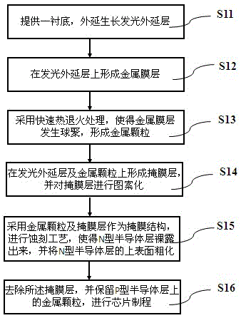
[0033] This embodiment provides a method for manufacturing gallium nitride-based light-emitting diodes. For specific procedures, please refer to figure 1 , including the following process steps:

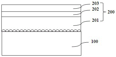
[0034] Step S11, providing a substrate, and epitaxially growing a light-emitting epitaxial layer.

[0035] Step S12, forming a metal film layer on the light-emitting epitaxial layer.

[0036] In step S13 , a rapid thermal annealing treatment is adopted to cause the metal film layer to spheroidize to form metal particles.

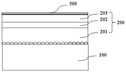
[0037] Step S14 , forming a mask layer on the light-emitting epitaxial layer and the metal particles, and patterning the mask layer.

[0038] In step S15 , using the metal particles and the mask layer as a mask structure, an etching process is performed to expose the N-type semiconductor layer and roughen the upper surface of the N-type semiconductor layer.

[0039] In step S16, the mask layer is removed, and the metal particles on the P-type semiconductor layer...


PUM


Abstract

The invention discloses a manufacturing method for a light emitting diode. The manufacturing method comprises the following technological steps of providing a substrate, performing epitaxial growth of a light emitting epitaxial layer which is formed by an N type semiconductor layer, a light emitting layer and a P type semiconductor layer in a stacking manner, and defining the upper surface of the light emitting epitaxial layer into a P type region and an N type region; forming a metal film layer on the light emitting epitaxial layer; performing quick annealing treatment to enable the metal film layer to be subjected to sphere agglomeration to form metal particles; forming a mask layer on the light emitting epitaxial layer and the metal particles, and performing patterning on the mask layer to expose the N type region; taking the metal particles and the mask layer as a mask structure, performing an etching process to etch the N type region until the N type semiconductor layer is exposed, and performing roughening on the upper surface of the N type semiconductor layer; and removing the mask layer, reserving the metal particles on the P type semiconductor layer, and carrying out chip processing.

Description

technical field [0001] The invention relates to the technical field of semiconductors, in particular to a method for manufacturing a light emitting diode. Background technique [0002] After years of development of light-emitting diodes (LEDs), III-V compounds are currently the mainstream semiconductor materials for making light-emitting diodes, among which gallium nitride-based and aluminum gallium indium phosphide-based materials are the most common. Generally, the external quantum efficiency of gallium nitride-based LEDs depends on its internal quantum efficiency and light extraction efficiency. The internal quantum efficiency of most commercial LEDs is close to 100%, but its light extraction efficiency is only about 3-30%. The most important factor is the loss of photons generated inside the LED due to internal total reflection. [0003] The roughening of the LED interface can effectively improve its light extraction efficiency. One of them is the combination of ICP dr...

Claims


Application Information

Patent Timeline
IPC IPC(8): H01L33/22H01L33/14H01L33/00
CPCH01L33/005H01L33/14H01L33/22
Inventor 夏章艮王锋林素慧彭康伟洪灵愿徐宸科
Owner HUBEI SANAN OPTOELECTRONICS CO LTD
Why Eureka
Try Eureka